 |
First thing we need for efficient LED's and Lasers is a large quantum efficiency, that is a high percentage of radiative recombinations. Since this is so
important, let's repeat some of what we have already covered in the sub-chapter
before this one. |
|
 |
In more elementary semiconductor materials science we learned that in direct semiconductors a recombination event happens if an electrons in the conduction band meets
a holes from the valence band; the pair recombines and emits a photon. Let's call that process now direct
recombination or band-band recombination- and yes, a photon will still
be emitted. |
 |
There is one other recombination channel that you have already learned about:
recombination via defects in indirect semiconductors or defect recombination.
We might distinguish point defects in the bulk acting as recombination center,
dislocations or interfaces - they all have one thing in common: They introduce some defect levels usually deep in the bandgap
(so-called "deep levels"). |
|
 |
Recombination happens because these deep levels can be
occupied by electrons and holes. In a simple visualization as shown below, the deep level captures an electron and within
time constraint a hole, too - the net effect is the disappearance of an electron-hole pair, i.e. recombination. |
 |
Now we must look at even more more recombination mechanisms, or recombination channels as we will call it now, then you have not encountered so far (don't overburden
the freshmen and -women!). |
|
 |
We have, for example, recombination via defects not only for indirect
semiconductors. There is no reason why it should not also happen in direct semiconductors.
This recombination channel then is in competition to the direct recombination but will not
produce photons. |
 |
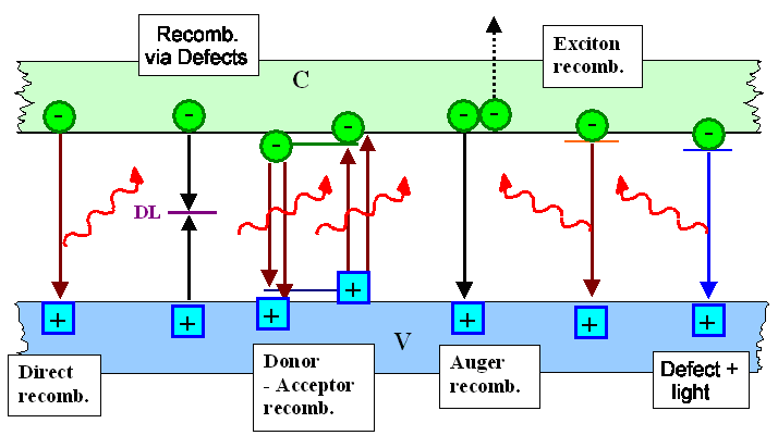
The picture below shows a lot more possible recombination channels,
all applicable to direct semiconductors, and we cannot possibly understand all of them in detail at present (more to this
topic can be found in this link). However, we can try to appreciate
a few basic points:
- In direct semiconductors there are a number of recombination channels that do not produce light - in particular defect based non-radiative recombination (prominent if there
are many defects) and "Auger" recombination (prominent at very high carrier
concentrations). That is bad.
- In indirect semiconductors we may find radiative recombination channels - in particular
via "excitons" or some special defects. The former is responsible for the use
of GaP - an indirect semiconductor - as material for green
LED's, the latter for light coming out of SiC; also an indirect semiconductor.
This is good.
|
|
|
|
 |
A high quantum efficiency calls for having mostly radiating
recombination channels, and that calls for optimizing the material you have according to its peculiar specifics, your technological
potentials, and perhaps your budget. |
|
 |
It is not necessarily an easy task. That it can be done at an impressive level
for some semiconductor materials is demonstrated by the fact that we have working and affordable high-efficiency LED's
right now. |
|
 |
How far this can go, in particular with completely new materials like organic
semiconductors out there, remains to be seen. |
|
| |
|
Getting
the Light Out |
| |
|
 |
Unfortunately, a LED generates light inside
the semiconductor where we don't need it. We must get the light out in the air, preferably with some defined radiation characteristics.
|
| |
|
 |
Look at you electronic gadget from somewhere in the room. If you want to see
if it is "on", the (usually) green light generated inside the GaP
LED must come out. Preferably in the shape of a rather large cone as measured with some spherical angle. The first
priority, however, is to get the light across the semiconductor - air interface at all. |
|
|
|
 |
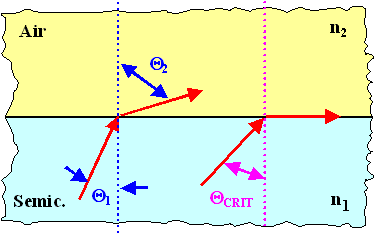
Remembering Snell's
law from basic optics, and knowing that n1 = index of refraction
of air = 1, we have with respect to the situation shown in the picture |
|
|
| |
|
|
|
| |
|
| |
|
 |
As also shown in the picture, total (internal) reflection will happen if sinQ1 = 1/n2. Considering that n2 = index of
refraction of the semiconductor » 3 - 4, only light emitted towards the surface into
a relatively small cone will be able to "come out" at all. |
|
 |
This is not good and causes a serious problem for high efficiencies. A lot of
the light produced will simply not be able to come out into the air, and some of the light that makes it will be in the
wrong direction (e.g. "backwards"). We must employ some optical engineering
at this point. |
| |
| |
|
 |
As always, there are simple and more complex ways to solve the problem. |
|
|
|
 |
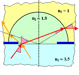
A very simple and cheap solution is shown in the picture. The idea is not to allow large jumps
in the refractive index across a boundary but to use index grating. |
|
|
 |
Just one intermediate layer with an index n3 between n1
and n2 may already provide a big improvement. In a simple version with wide-spread application,
just adding a "dome" of some epoxy as shown will not only get more light out of the semiconductor, but will also
distribute it more or less evenly in a large steric angle - exactly what you want for the little signal lights of your gadgets. |
|
|
| |
| |
 |
There is one more problem, however. While we may now be able to get
most of the light out that reaches the semiconductor surface, we still have the problem of getting the light there in the
first place. Considering that light might be generated deep inside the semiconductor, we must take into account that it
will be absorbed again before it reaches the surface. |
|
|
|
 |
After all, the energy of the light generated comes from the recombination of
an electron and an hole, the energy of the light thus by definition is just what is needed to generate an electron-hole
pair. | |
|
|
 |
In other words: A run-of-the-mill digital camera, operating
with a Si "CCD"
chip that detects light by generating electron-hole pairs in Si, will also detect the (little bit) of light produced
by very good solar cells under open circuit condition after a lot of electron hole pairs have been generated by a high intensity
light flash. Even so Si is an indirect semiconductor, if you block its usual defect recombination channels, which
you do by definition in a very good solar cell, some radiative recombination will occur and detecting it will tell you a
lot of what is going on inside your solar cell. | |
|
 |
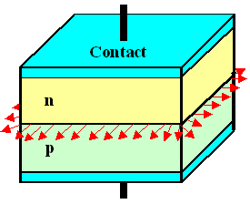
In yet other words: if we just make a pn-junction as shown in the picture
in order to produce a simple LED, we get some light from around the edges (in all directions; not shown), but most
of the light generated in the interior will never make it to the outside world. |
|
|
 |
There seems to be no easy fix for this problem. Indeed - there isn't, as long
as we use only one type of semiconductor. However, if we now turn to hetero
junctions, we can solve this and other problems very elegantly - and acquire new problems in the process. |
|
|
| |
| |
|
Recombination Volume and Hetero Junctions |
| |
|
 |
The problems pointed out above together with some other considerations make it
clear that we must have control over where exactly the light is generated. |
|
 |
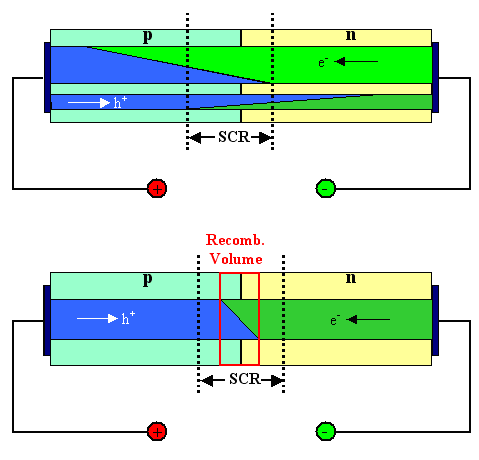
If we make just a regular pn-junction and run it under forward bias, we
inject a large forward current of electrons and holes from the n- part and the p-part of the junction into
the other side, respectively . As soon as our majority carriers cross the junction, they become minority carriers and start
to recombine with majorities. |
|
 |
This is shown schematically in the upper half of the picture below. The small
reverse currents have been omitted, and it was assumed that the n-part is more heavily doped than the p-part
(can you tell how?). |
|
 |
Recombination happens inside and outside the space charge region (SCR) as shown; the exact
geometry is given by the life time, the corresponding diffusion length, and God (actually rather Shockley,
Read and Hall) knows what else. We have already looked at recombination
inside the SCR in a simple-minded way, found that it might be substantial, and that it may even be dominating
in semiconductors with bandgaps > 1 eV or so. |
 |
We might expect therefore that most of the light will be generated in the SCR,
but we want to do better than that. We want to determine exactly where the light is produced - in a recombination zone that we want to make to specifications. |
|
 |
What that might look like is shown in the lower part of the picture. Again we
inject large currents of electrons and holes across a junction with some SCR, but they all recombine within a defined
recombination zone that is smaller than the SCR. The two injection currents are shown as just one current in this
case. |
| |
|
 |
As already mentioned, we can do all this by using hetero
junctions. We then also enter a rather difficult part of semiconductor physics, and we can not go into much details
here - activate the link if you want to learn more. |
|
 |
We will just ask two simple questions and look at the answers without doing the
reasoning necessary to derive those answers. |
 |
1. How do we construct a pn-junction between two semiconductors
with different bandgaps? |
|
 |
The answer is: Exactly
as before for a homo junction. However, we encounter a problem: There must be a discontinuity of the conduction and valence band right at the (metallurgical)
junction - and we don't know how to deal with that. |
 |
2. What happens if we form a junction between two semiconductors with different
bandgaps but of the same doping type - a Pp or nN junction (with capital P and N denoting the
semiconductor with the larger band gap)? |
|
 |
The answer is: same procedure as
before: Align the Fermi energies, consider that far away from the junction nothing has changed, move electrons and holes
at the junction to the part where their energy is lowered, consider the charge and the associated band bending ... . But
again, there must be a discontinuity now, and we don't know how to deal with that. |
 |
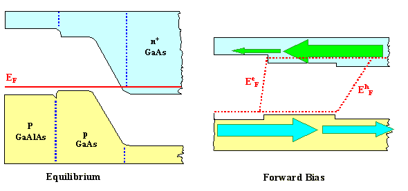
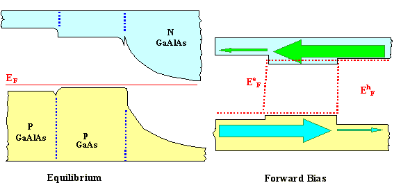
Cutting a long (and involved) problem short, below are some band diagrams of typical
hetero junctions. The necessary discontinuity in the energy has been split into a DEC
and a DEV "somehow". |
|
 |
Shown are both cases: a Ppn - single hetero junction and a PpN double hetero
junction in equilibrium and under extreme forward bias with electron and hole currents indicated. |
|
 |
For the forward bias case the Fermi energies in a strict sense do no longer
exist (they are equilibrium properties, after all); instead "Quasi Fermi energies"
are drawn in that need not concern us here, but are explained in this link. |
| |
|
|
 |
What
we are interested in is the PpN device with two junctions, biased in forward direction. In this case we inject
a large electron current from the N part into the p part, and a large hole current from the P part
into the p part - just as in the case of the single hetero junction. The difference is that these currents cannot
easily get out on the other side of the small bandgap semiconductor because we have an additional energy barrier now |
|
 |
If the electrons and holes injected into the small bandgap semiconductor from
the two wide bandgap sides cannot get out, their only way to oblivion is to recombine in the small band gap semiconductor. |
 |
Let's see what we have achieved:
- All the electrons and holes injected via forward bias must recombine in the volume of the small bandgap semiconductor
- they can get in, but not out! We now have a defined recombination volume.
- The light generated in the recombination volume can easily move into the large bandgap semiconductors because there
is no large difference of the index of refraction. And in these semiconductors it will not be absorbed
at all for obvious reasons.
|
|
 |
We have now solved all the problems mentioned above - and generated the following new problems:
- We now have phase boundaries between different crystals, which
we have to keep free of defects, in particular we must avoid misfit dislocations. That severely limits the choice of materials.
- If we use a semiconductor like GaN to generate UV light as the "small bandgap semiconductor",
there is not much choice anymore for the "large" bandgap semiconductors.
- Ohmic contacts to large bandgap semiconductors (that we still need, of course) are notoriously more difficult to make
than to small bandgap semiconductors.
- More involved technology increases costs.
|
| | |
 |
All things considered, we see that there is far more to making a decent LED
from some direct (inorganic) semiconductor than just making a pn-junction. The field is still progressing rapidly,
and only time will tell what we are going to "see" in a few years from now. |
| |
|
Molecular
Beam Epitaxy |
| |
|
 |
So far we have already encountered two examples - one,
two - of devices where lots of thin layers of different
semiconductors were stacked on top of each other; another one will come up |
|
 |
The question is - how is it done? How do we make complex successions of thin
layers from different materials with various thicknesses and doping? Are we going to use variants of the CVD process
that we used for epitaxial Si? |
|
 |
No - we won't. it would be too cumbersome and slow to grow one layer, then to
change gases and whatnot for the next layer, always hoping that all parameters are just right and that no cross-contamination
occurs. We use molecular beam epitaxy or MBE, the universal tool developed for just this task |
 |
The principle of MBE is simple. Suppose you want to make 84 nm thick
layer of Ga0.8Al0.sAs doped with 5 · 1017 of Si on a plain GaAs
substrate. All you have to do is: |
|
|
- Keep your substrate with an atomically clear surface at some suitable temperature.
- Direct a low-energy flow of all the atoms (or small molecules) needed with just the right rate - atoms per second and
cm2 - on your substrate.
- Let 'em react right on your substrate to what you want. They actually have no choice in this example. Each atom will
occupy just right position as soon as it is chemisorbed
on the substrate.
- Stop the process suddenly as soon as the required thickness is reached.
|
 |
So the principle is easy, the technology, unfortunately, is not. Let's see what
we need and how we can meet these needs. |
|
 |
The first point clearly calls for ultra-high vacuum (UHV), a heater with temperature control, and some way to clean the surface after the substrate
is in place. This can be done, for example, by blasting off (ever so gentle) the surface oxide or whatever you have with
an Ar ion beam |
|
 |
There is no real problem here - provided you have the cash to pay for UHV,
a notoriously expensive undertaking |
|
 |
The second point first of all calls for very
low flow rates because you want each atom to go only to the substrate - no interaction with all the other atoms going there
on the way. This means you must keep the concentration low or, in other words, the mean free path length very large. Nevertheless,
the low flow rates still need to be precisely controlled - and now we have a problem: how do we achieve that for all kinds
of atoms? |
|
 |
By designing sources called "effusion cells"
or "Knudsen
effusion cells" The word "effusion" is reminiscent of "diffusion"
but the meaning is different. Effusion means "pouring forth" or, according to the Webster:
"the escape of gases through minute apertures into a vacuum. That is exactly what an effusion cell does: Provide and
keep a very well defined vapor pressure of the material in question inside a "container" and let a defined amount
of the vapor escape through a suitable orifice. The key word is "defined" because MBE needs to be a high
precision technique. Obviously, out MBE machine needs several effusion cells; each one optimized for, e.g. Ga,
As, Al and Si. |
|
 |
The third point is simple now. All we have
to do is to make sure that we have the same rate of incoming atoms everywhere on the substrate (not
easy for large wafers!) and that the substrate has the optimal temperature to enable the various bonding processes that
have to occur on its surface. |
|
 |
The fourth point is not so simple. We need
to incorporate some in-situ technique that monitors the thickness of the growing layer without interfering with the growth
process, and we need some way to stop the process. The latter requirement is easy: Just close the orifices of the effusion
cell by some mechanical shutter - except that mechanical movements in an UHV are not all that simple. |
|
 |
The in-situ measurement of choice is mostly "RHEED"
or "Reflection High Energy Electron Diffraction". The name says it all, and we won't elaborate on this |
 |
Taking everything together, a MBE system is a fairly complex piece of equipment
but central to many branches of semiconductor technology. The link provides
some pictures and a few more details |
|
 |
Of course, for serious production you try to find solutions that are less complex
and expensive and geared to one process only. |
© H. Föll (Semiconductor Technology - Script)
