 |
The bulk-Si solar cell was called "bulk"
because its thickness of > 200 µm is far larger than the thickness of the space charge region in the necessary
junction. | | |
 |
There are two reasons why we make these bulk-Si solar cells:
- Infrared and even red light may penetrate Sito a depth of many µm. In fact, Si membranes with
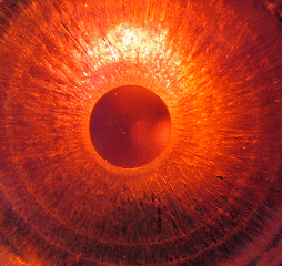
a thickness of just a few µm are somewhat transparent even in visible light as shown. If we want to absorb as
much light as possible we must use "bulk" Si.
- If we use a thickness of > 200 µm, the solar cell is self-supporting (even so it breaks easily) and we
do not need a substrate.
| |
 |
Backlit polycrystalline Siwith a thickness
around 5 µmshows some transparency
in the red. |
|
|
 |
The catch is that we need a lot of expensive Silicon. |
|
|
 |
Class Exercise:
How much area in m2 and how many kg of Si do you need for a 1 GWpower
plant. Assume an efficiency l=15 % and that the average power delivered is 12 %
of peak power. | |
 |
This gives us some (connected) major conditions for making thin film solar cells.
- The semiconductor should have a suitable direct band gap Eg
» 1.5 eV since this ensures high absorption coefficients for all light with hn > Eg and high efficiencies.
- There must be a process-compatible and cheap substrate on which we can deposit the thin layers.
- Since perfect single crystalline layers are impossible under the circumstances, "defects" in the layer and
its interfaces must be harmless with respect to recombination.
- There must be some efficient (and cheap) way to produce a junction and decent ohmic contacts.
|
|
|
 |
Those are tough requirements. While some (which ones?) are valid for all
solar cells, they might be considered very special for a given thin film system. |
|
|
 |
We certainly have enough semiconductors to chose from - remember this link?
So far, however, only a few semiconductors have made it - in the sense that you can find them in the form of solar modules
on roofs. A few more can be found in laboratories, but all in all the list is rather short. |
|
 |
Major thin film solar cells belong to one
of the groups given below: - Amorphous Si.
- Nanocrystalline thin film Si.
- Polycrystalline thin film Si.
- The CuInxGa1-xSe2 or "CIGS" family.
- The CdTe solar cell.
- The TiO2 - dye based family.
- Multi-layer based tandem cells or multi-junction cells.
- Exotica.
|
 |
If you feel that points 1 - 8 could be seen as the table of contents for
a complete lecture course - you are right. Indeed, there would be a lot of ground to cover if we just were to look at the
basic research, develeopment and - where already applicable - production of the thin film solar cells enumerated above.
To give just one example of the complexity encountered: |
|
 |
Why is "CIGS" better than just "CIS" (=CuInGaSe2)? Why are traces
of Na important for making good CIGS solar cells? Why is Mo the best metal for the backside contact?
Will there be enough In available for making CIGS cells in a big way? Why are properly made CIGS solar
cells quite immune to radiation (as encountered by satellites in space)? Why are the recombination properties of the CIGS
layer rather insensitive to its production method (sputtering, CVD in many variants, galvanic deposition, sintering,
...; everything seems to work)? What are the major limits to the efficiency? How stable is the combination of the many materials
found in a CIGS cell over decades? |
 |
All we can do here is to give a short summary of what is meant with the catch
words in the list, and to look at a few essentials of production methods for thin film solar cells in the next sub-chapter.
In time, advanced modules may spring into existence with additional information to each type of thin film solar cell. |
| |
|
Amorphous Si Solar Cells |
| | |
 |
Amorphous Si or a-Si solar cells are almost as old as crystalline
(or c-Si) solar cells. It is rather easy to produce thin film amorphous Si - just sputter from a Si
target, or use Si-CVD at temperature < » 400 0C. A layer thickness
of 1 µm or less is enough to absorb all light and thus we are truly talking "thin film" here. |
|
 |
However, pure amorphous Si is a good insulator and rather useless because it contains
by necessity many "dangling bonds" that introduce electronic states in the
band gap in a high density. Only if we "passivate" these dangling
bonds with hydrogen (H) do we become a halfway decent semiconductor that
behaves like a direct semiconductor with a band gap of about 1.7 eV. |
|
 |
Now we have the first mystery about "amorphous Si". While the density of
dangling bonds is large but still well below 1 % of all bonds, we need to put 5 % - 30 % hydrogen into the
material to achieve decent semiconducting properties, i.e far more than we would need for just compensating the dangling
bonds. In fact, what all and sundry calls "amorphous Si" is actually an amorphous Si-hydride; the
abbreviation a-Si:H is often used. |
 |
Eschewing these "details", we are left with a material that behaves in many respects roughly
like Si, can be doped n-type and p-type, comes relatively cheap, and can be handled to a large extent
by existing Si technology. It also can be deposited on large-area substrates. |
|
 |
We thus can produce solar cells, e.g. on a glass substrate. Contacts are a problem, but neglecting
that for a moment, a-Si:H solar cells have been plagued from the very beginning by some specific problems that have
not gone away even after decades of R&D:
- The efficiency h is rather low ( <» 10 %
to give a number) for various reasons, and not easily (=cheaply) raised. For serious power application this is bad - being
cheap at some point does no longer compensate for low efficiencies.
- a-Si:H solar cells are prone to show the so-called Staebler-Wronski effect,
i.e. their efficiency h degrades by up to 30 % if the solar cell is exposed to
light for some time!
- The efficiency recovers upon heating the solar cell, but that is of little use. What exactly causes the Staebler-Wronski
effect is a matter that has been intensively investigated for > 20 years, but the final word is not yet in.
|
|
 |
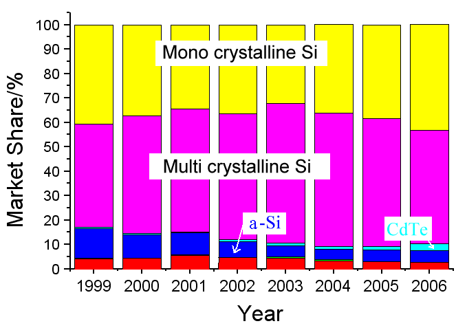
Nevertheless, a-Si:H solar cells do have a noticeable market share as shown below: |
| |
|
|
 |
Note that a constant market share still means substantial
growth in absolute numbers if there is substantial market growth - which we do haeve!
Also note that beside a-Si:H solar cells, and lately CdTesolar cells, all other thin film cells hold only
a miniscule market share (CIGScells are shown in green; the red part denotes "RGS" - ribbon growth on substrate,
a variant of Si solar cell technology). |
 |
You probably own a-Si:H solar cells - in your pocket calculator, your watch,
or in other small electronic devices where the efficiency (and durability) is not cricitical, but size, weight, price and
easy production compatibility are important. |
|
 |
While there are also some large scale applications, it is not clear at present if a-Si:H
solar cells will play a big role in the future. |
|
| |
|
Nanocrystalline Thin Film Si Solar Cell |
| | |
 |
While nowadays everything either just small or complex goes as "nano this-or-that",
solar cells made from truly nanocrystalline thin fim Si is actually called "micro-crystalline Si" or µc-Si:H in most publications. |
|
 |
Be that as it may, the fact is that it became clear some 6 years ago that thin layers
of Si that actually consist of Si nanocrystals (diameters in the 10 nm region) embedded in a a-Si:H matrix (still containing plenty of hydrogen), if made exactly right, could be used to make
solar cells with efficiencies of up to 14 % and with practically no Staebler-Wronski effect. |
|
 |
That gave a big boost to the many researchers engaged with a-Si:H solar cells since
it offered a new outlook to the future of these solar cells. |
|
 |
What exactly makes the µc-Si:H thin films so much better than just a-Si:H,
and how far this can be carried, is not all that clear at present. |
 |
To the best of my knowledge, there are no nanocrystalline thin film Si
solar cells up on roofs in a major way at present. If this kind of thin film solar cell will make it into large scale production,
is an open question at present, but it is seen as a major future contender for the presently firmly entrenched bulk Si solar cell.
|
|
Multi-crystalline "Thin" Film Si
Solar Cell |
| |
|
 |
Make a bulk mc-Si solar cell with just about (2 - 5) µm thick
multi-crystalline Si. It will not absorb all the light, so add a "mirror" at the back and other measures
to keep the light inside the Si. |
|
 |
This would work quite well - except that you can neither make 5 µm thin slices,
nor handle them without fracturing them rather quickly. |
|
 |
So put your 5 µm, or even just 2 µm, of larged-grained or "multi-crystalline
(mc)Si on a mechanically (and thermally) stable substrate. This is the concept of the "thin film Si" solar cell as it is usually called. |
 |
There is no uncertainty about possible high efficiencies, long life times without
degradation, etc. - it's good old and well-known Si technology after all. The problem, alluded to many times by now
is: money. |
|
 |
In other words, you are competing aginst good, old, and well-known bulk Si technologies
- and you must be just as good and considerably cheaper before you are being noticed. So you must solve the follwing problems:
- Deposit rather thick layers of rather good Si (pure, large-grained, ...) quickly
(at least 1 m2/min). Normal Si CVD processes are not that fast, and tend to produce small-grained
films.
- Find a cheap and process-compatible substrate.
- Think about the temperature budget. While the Si part would be easier at high temperatures (deposition rates
go up, grains grow larger, ...), you better stay at low temperatures all the time - or you will be very restricted in the
choice of your substrate (heating also costs money).
- What about the backside contact if that cannot be your substrate (because you picked glas)?
- And what about the backside "mirror"?
- And so on and so forth.
|
|
 |
Impressive progress has been made with the thin film Si solar cell. If it will become
competitive in the near future remains to be seen. |
|
The CIGS Solar Cell |
| | |
| |
 |
Solar cells from the CIGS family have an "old"
history - it goes back more than 20 years to the times around the first oil crisis (1975), when semiconductors
of the metal1-metal2-chalgogenide family were studied with some effort.. |
|
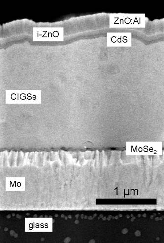
 | Cross-section through a CIGS cell
Copyright Hahn-Meitner-Insituts, Berlin |
|
|
 |
One of the first promising materials contained mercury (Hg), and since
mercury acquired a really bad name in those days, there were reservations about these materials, too. This might be about
as smart as having reservations about NaClbecause both Na and Cl do belong to the terrorist group in
the periodic table. | |
|
 |
Anyway, with lots of research it became clear that the "CIGS" 'family showed
real promise. Serious production started around 2005, and by now the first large
factories are up and r unning. | |
 |
Some topics around CIGS solar cells have already been raised above. Here we note that having an (always p-doped) CIGS layer of about (1 - 2) µm
in thickness is not enough, we also need a pn-junction and (low resistivity) contacts. |
|
|
 |
The pn-junction is actually a hetero junction;
the n-part is supplied by a very thin layer of CdS and intrinsic (=high resistivity) ZnO. The backside
metal is Mo, possibly reacting with the CIGS upon deposition to a thin intermediate layer of MoSe2
as shown above. | |
|
 |
Heavily p-doped (with Al) ZnO forms the transparent contact layer on
top. The not-so-great resistivity of the top layers causes problems that will be dealt with in the next
sub-chapter. Just take it for granted at that point that the simple technique of screen printing some metal contacts, as known from bulk Si solar cells, does not work here. |
|
 |
Anyway, after many years of R&D, we have almost 20 % efficiency
CIGS cells in the laboratory and around 13 % in mass production. |
|
|
 |
Also, after many years of R&D, we still have some "black art" involved in making CIGS solar cells. In the words of the Hahn-Meitner-Institut
in Berlin, one of the leading CIGS R&D places: | |
| |
"Despite the large CIGS progress made in the last 10 years, the material science (of
CIGS) is still behind that of established semiconductors like, e.g., Si. Progress in increasing the efficiency by semi-empirical
optimization of the physical and chemical processing steps was essential for success. In other words: 'It worked first and
was explained later'" | |
 |
Since CIGS solar cells have the potential for good efficiencies around
20 % and cold be potentially cheap, they are seen as the major competitor to the Si bulk cell right now. Time
will tell. | |
| |
| |
|
The CdTe Solar Cell |
| | |
 |
CdTe solar cells have a bad image right now (around 2007) because
they use Cd, one of the more despicable elements in present mythology (possibly belonging
to the terrorist group of the periodic table). |
|
 |
However, CdTe solar cells are relatively easy to make, not too bad, and
rather cheap. The real problem comes from the fact that all of the solar cell industry must consider how to recycle their
products eventually - and that might be not so cheap with Cd containing waste. |
|
 |
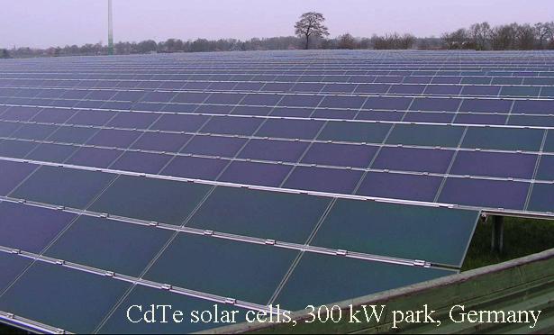
Beside image problems, a real problem might be that the efficiency of CdTe solar cells
might be limited to values not competitive in future markets. There are, however, already large-scale installations as shown
below. Again, time shall tell if CdTe solar cells are here to stay. |
| |
 |
| 300 kWp solar park with CdTesolar cells made by Antec; in Aurich, Germany
|
|
 |
Feb. 2010: Time did tell. First Solar, making exclusively CdTesolar
cells, is now the biggest solar cell company on the planet. |
|
 |
Thin film CdTe solar cells enjoyed a tremendous success story in just a few years.
The concern now is rather if there is enough Te around to allow many GW of installations. |
| | |
|
|
The TiO2 - Dye Based Family |
| | |
 |
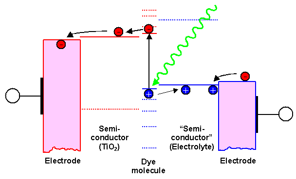
The basic idea behind this solar cell concept is best illustrated in a schematic
band diagram |
| |
|
|
 |
We use an optimized dye molecule that absorbs light extremely efficiently, and in doing so kicks
an electron up from the highest occupied molecular orbital (HOMO-level;
shown as solid blue line) to the lowest unoccupied molecular orbital(LUMO-level).
In semiconductor terms an electron-hole pair is generated; in more general terms we have an exciton (=electron-hole pair
at close range, feeling some interaction). |
|
 |
The trick is to separate the two carriers. If we find suitable semiconductors that have their
conduction band just right below the LUMO level (so the electron can jump over with some energy gain) or their valence
band right above the HOMO level (so the hole can jump over with some energy gain), respectively, and some metal electrodes
with suitable Fermi levels - we have a solar cell. |
|
 |
Well, not quite, because at least one side needs to be transparent to light. In this case
it will be the hole side, where Indium-Tin-Oxide commonly known as "ITO" works well enough. On the electron side we can use TiO2
and some metal with a lot of advantages as we will see. |
 |
The problem is the blue "hole" semiconductor. It must alos be transparetn
to light - and presently there is no good candidate. The so-called "Graetzel"
cell, the paradigm of this kind of cell, therfore uses a "redox" electrolyte that can transport the electrons from right to left (akin to transporting a hole from
left to right) at the proper energy levels. |
|
 |
The big advantage of the Graetzel cell (and its many
variants) is that the TiO2 + dye side is very simple and dirt cheap: Take TiO2 nanoparticles,
sinter them lightly onto a metal substrate, and coat the resulting nano-sponge with the dye. TiO2 nanoparticles
dispersed in some solvent, in case you don't know, is what you buy as "white paint" in building supply stores
- it is truly cheap. |
|
 |
The dye might be a problem, but organic chemistry will solve it for you. It may not be dirt
cheap but you only need tiny amounts. |
 |
The real problem, of course, is the electrolyte side, in particular if it is supposed
to work for > 20 years without a problem. |
|
 |
The Graetzel cell holds a lot of attraction for many R&D oriented people and organisations.
It doesn't require expensive semiconductor equipment to start experiments, and it offers a chance for researchers from various
disciplines other than semiconductor materials science to try their hand at solar energy. It is therefore small wonder that
some "Graetzel cell" concept has been touted as the solution to
the problems plaguing solar energy every few years since the eighties. |
|
 |
However, the few efforts at large-area semi-commercial Graetzel cells invariably did not result
in industrial production. One problem is that efficiencies are well below 10 % at present - and that is just not
good enough. Another problem is the required massive series connection, which is just not that easy if liquids are involved.
|
|
 |
Nevertheless, given the large number of researchers and institutions working on some variant
of this cell concept, the final word is: Time will tell. |
|
| |
|
Tandem or Multi Junction Cells
|
| | |
| |
 |
It was emphasized many times that with a given band gap the efficiency
of a solar cell is limited, and that the "best" bandgap for sunlight would be about 1.5 eV, giving a maximum
efficiency of about 30 %. | |
 |
| Courtesy ISE, Freiburg |
|
|
 |
How about using solar cells made from semiconductors with different bandgaps,
stacked on top of each other? The first one, facing the light should have a wide bandgap, taking out just the ultraviolet
part of the spectrum. It will generate a relatively high voltage and some current. |
|
|
 |
Below the first layer then sits a medium bandgap solar cell, responding, let's say, to yellow
and beyond. It would generate a medium voltage and some current. |
|
|
 |
Finally, in the triple junction solar cell
we are generating, we have a small bandgap semiconductor absorbing the left-over red and infrared radiation; generating
a small voltage and some current. | |
 |
We see the first problem of our high-efficiency
multi-junction solar cell: we need current matching! The current generated in the individual cells must flow through all three cells
since they are switched in series. If the three cells do not generate the same amount of current, we will have problems. |
|
|
 |
Current matching can be achieved if the thickness of the
individual layers, the bandgaps, and so on, are matched to the solar spectrum. Tedious, but possible. |
|
|
|
Class Exercise:
What would happen if there is no current matching? It is sufficient to consider a tandem cell with
two junctions. | |
|
 |
If we made sure that we haev current matching, the individual cell voltages will add up and
we may have an efficiency exceeding the maximal 30 % for single junction cells. For example, with Ge as the
"bottom cell", and plenty of other cells on top (¥ many with incrementally
increasing bandgap for "easy" theory), the theoretical limit is > 50 %. |
|
 |
However, besides current matching, we must solve another problem. If we pile many
different semiconductors on top of each other, the interfaces should better be "good" in the sense of not recombining
carriers. In other words: no misfit dislocations. |
|
|
 |
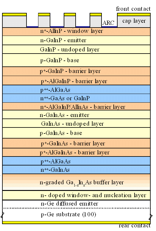
That narrows done the possible combinations but we still can do quite a bit - as shown in
the figure. The band gap goes up in steps from the 0.66 eV of Ge to about 1.8 eV of the GaInP. |
|
|
 |
The misfit is kept small, and experimental efficiencies in excess of 40 % have been
obtained | |
|
| |
| |
 |
The catch is obvious: Multi-junction solar cells will not come very cheaply! There
is no way to make m2 of this structure in an inexpensive and fast way. This leaves two escape routes: |
|
 |
1. Make far simpler structures - e.g. a simple variant of a tandem cell,
e.g. by just using a-Si:H on top of a-Si/Ge:H. Instead of using amorphous p-Si as absorber, alloy some
Ge into this layer, lowering the band gap. On top put regular n-type amorphous Si with a larger band
gap. This will not give you "high efficiency", but possibly more than just a simple a-Si:H solar cell.
Or use n-type a-Si:H with is relatively wide band gap on top of crystalline bulk p-type Si.
Or --- you get the idea. |
|
 |
2. Make the best multi-junction solar cell you can, and put it in the focus
of some parabolic mirror, or any other cheap focussing device like Fresnel lenses. In other words, concentrate the sun light
collected from a large area on a small area solar cell - which then can be expensive. This is the principle of the concentrator solar cell with the obvious catch that it will only work in direct sun light (i.e. not
in my home state of Schleswig-Holstein, where we might not see the sun for weeks on end) and
and if some mechanical contraption follows the sun. |
 |
There is definitely a market for concentrator cells; how large it is remains to
be seen. |
| |
|
Exotica |
| | |
 |
Even the most stupid American (G.W. Bush?) realized by now (2007) that it is time
to worry about the climate and about the finite resources of cheap energy carriers like
oil. This means that the USA are just now (re)discovering solar energy. Since they almost completely missed the big
economical boom of solar energy after the year 2000, they are lacking behind in solar cell production but have now
taking the lead in solar cell hyperbole. |
|
 |
Check the Internet. Tip: Start with "nanosolar". You will find all
kinds of new concepts for making cheap and very good solar cells. However, as the saying goes: "the proof of the pudding
is in the eating" - or time will tell. |
 |
There are, however, many more serious "exotic" solar cells concepts
in the sense that they are either considered or actually used for very special applications (like supplying power to satellites),
or objects of intensive R&D. |
|
 |
In the first category we have all kinds of GaAs based solar cells - optimal
band gap for best efficiencies of single junction cells; used whenever price doesn't matter (in space). |
 |
In the second category we have, for example, solar cells based on organic semiconductors. |
|
 |
Light emitting diodes (electric power in; light out) made from organic semiconductors are
already on the market; so the inverse device (Light in; electric power out=solar cell) should be possible too as seen from
a somewhat naive point of view. |
|
 |
Yes, organic solar cells are possible. Right now, however, they are subject to a host of problems.
If those problems could be solved, leading to a potentially extremely cheap technology ("paint on your solar cell"),
only time will tell. |
| |
| |
© H. Föll (Semiconductor Technology - Script)
