 |
Bulk Si solar cells are made from (cheap) single crystalline wafers (cut
squarish) or from square multicrystalline (mc) wafers. They account for about 85 % of the installed solar power at present (2008).
| |
| Processing Time |
1s / solar cell |
| Cost Decrease | 5 % / a |
| Efficiency Increase | 20 % in 2012 ? |
| Key Material Supply | 30 % /a more Si |
Industry Growth Rates
> 30 % for many years |
Supply capital and people |
|
|
 |
A yearly production of 1 GWpeak means about 107
m2=10 km2 pn-junction of good quality and much more |
|
|
 |
Consider Þ |
|
|
|
A big problem is cranking up world wide Si production by 30 % - 40 %
per year. | |
|
| |
| |
 |
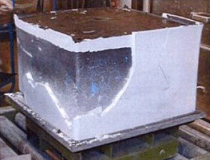
mc wafers are produced by Si casting. Problems are |
|
|
|
 |
Expansion upon crystallization. |
|
|
 |
Reaction with walls of mold | |
|
 |
Columnar grain growth required |
|
|
 |
300 kg ingots are routinely cast in 2007; liquid encapsulation and precise temperature
control are essential | |
 |
Sawing the ingot into mc-Si wafers with as little losses as possible and
with wafer thicknesses of < 300 µm, while straight-forward, is "high-tech". |
|
|
 |
Saw damage is removed by a chemical etch. |
|
| |
| |
| |
 |
Processing, simple in principle, has to meet the conditions above and is highly
specialized. Essential processes are: | |
|
|
 |
Diffusion, edge isolation, passivation, screen printing contacts and sintering contacts. |
|
|
 |
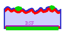
Essential device features are back surface field, gettering of impurity atoms, H-passivation
of grain boundaries and other defects. | |
| | |
|
© H. Föll (Semiconductor Technology - Script)

