 |
In semiconductor technology we make all kinds of thin films. Often, we make thin
films of some semiconducting material (cf. this picture) and then we want this
thin film to be a perfect single crystal with no defects whatsoever (except what we intentionally put in, e.g. for doping). |
|
 |
This is a tough job description. How can you make a single
crystalline thin film? Think about it. If you do it on a Si
substrate wafer with 300 mm diameter, you are actually demanding that any atom of your material B sitting
somewhere on your substrate, has a precise geometrical relation to any other atom being many centimeters away, for example. |
|
 |
You may think as hard and as long as you like, but the only way to do this is to deposit your
thin film on a single crystalline substrate to start with. If you are lucky, your B-atoms
then just continue the lattice of the A-substrate and you have epitaxial growth
or epitaxy for short. The term "epitaxy" comes from the Greek "epi"
meaning "above", and "taxis" meaning "in ordered manner".
|
|
 |
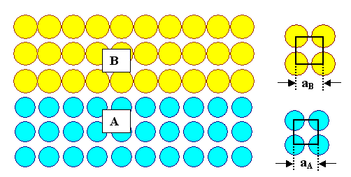
Let's look at a perfect epitaxial interface between A and B in a simple picture: |
| |
|
 |
That's what you want - but that is not what you will get. The reason is that we
must assume that the two lattice constants a of A and B are not
identical as shown on the right; we are lucky if the Bravais lattice types are. |
|
 |
In fact, it you look at our old "master
picture", summarizing the basic properties of important semiconductors, you see that the lattice constants of those
semiconductors are mostly quite different. |
|
 |
That leaves us with just two options:
- We may have a perfect epitaxial situation as shown above, but then we also have a lot of strain e
and stress s in our layer B, because we must squeeze it to fit on the substrate.
The strain energy stored in the stressed layer necessarily scales with e · s
and the thickness dz of the layer. Stress and strain scale with the misfit
f = (aA – aB)/aA of the situation,
i.e. the relative difference of the lattice constants.
- We will not have a perfect epitaxial interface.
|
 |
It's as simple as that. The question now is how much strain energy can a thin
film take before it is going to do a little stress relief by one means or another? |
|
 |
That depends on the means available fro stress relief. The most simple way of obtaining some
stress relief is to suffer some plastic
deformation, i.e. producing and moving some dislocations around. |
|
 |
This is exactly what will happen if the stress in a perfectly epitaxial thin film reaches
some critical value: the film deforms plastically and introduces what we call misfit dislocations.
A thin film may even do this if it cannot be plastically deformed as a bulk crystal like, e.g., Si. Misfit dislocations
are easy to visualize: |
| |
|
|
 |
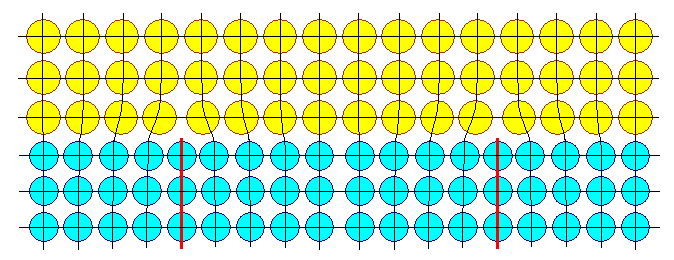
We have the same situation as above, but now we have misfit dislocations in the interface.
They must by necessity be edge dislocations (as indicated by the red lines),
or more generally, their Burgers vector must have
a sizeable component in the interface. |
|
 |
Obviously you must have dislocations at regular distances ddis (in
at least two directions - you will get a network) given by ddis = aA/f. |
 |
Now we have no more strain and strain energy in the thin film, but a lot of dislocations
in the interface. We know
or just believe that dislocations carry approximately the energy Edisl
= Gb2 per unit length (G = shear modulus). So what is better? |
|
 |
Same procedure every time. Look at the energy and compare:
- Perfect interface: The total strain energy scales with f · dz.
- Interface with misfit dislocations: The energy scales with the total dislocation
length or with the dislocation density, and thus only with f and not (or just a little bit) with dz.
|
 |
In other words: There is always some critical thickness dcrit
of the thin layer so that for dz > dcrit the introduction of misfit
dislocations in the interface is energetically favorable to having a strained layer. |
|
 |
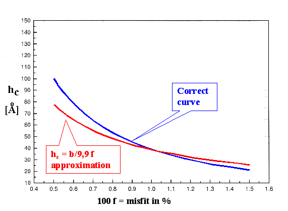
Going through the energy comparison in detail (not quite as easy as it looks) produces a very
important, very sad, and transcendent equation for the critical thickness; it is given below with a simple approximation
added. |
| |
| dcrit | = |
b
8p · f · (1
+ n) | · ln |
e · dcrit
r0 |
| | | |
| |
| dcrit |
» |
b
9.9 · f | |
|
|
|
|
 |
b is the magnitude of the Burgers vector, n =
Poisson's ratio, e = base of natural logarithms, r0 the "size" of the dislocation
core (about 1b). |
 |
Why is this a sad equation? Look at its graph. It shows the numerical solution
to the equation from above and the approximate solution. |
|
|
|
|
 |
It also shows, sadly, that the critical thickness is rather small if there is any misfit at
all. A misfit of just 1% will lead to an interface full of dislocations if the thin layer thickness exceeds about
4 nm! |
|
 |
It goes without saying, of course, that this is seriously bad.
If you don't know why, look at what you have learned
before. Defects like dislocations are never good news for electrons and holes in semiconductors. They reduce minority
carrier diffusion lengths and life times, the efficiency of light generation, and the product life time of Laser diodes,
for example. |
 |
You just can't have misfit dislocations in your electronically active semiconductor
- semiconductor interfaces. None whatsoever! |
|
 |
Now we understand why the lattice constant is the second important property besides the band
gap and plotted in our master picture, and why there are
so many combinations of semiconductors that we don't use. |
 |
Being engineers, we now ask ourselves if there are some tricks to beat the critical
thickness equation from above. The answer is: Yes - but you don't get very far at present. One of the neater ideas, going
under the heading of "compliant
substrates", can be accessed by the link. |
 |
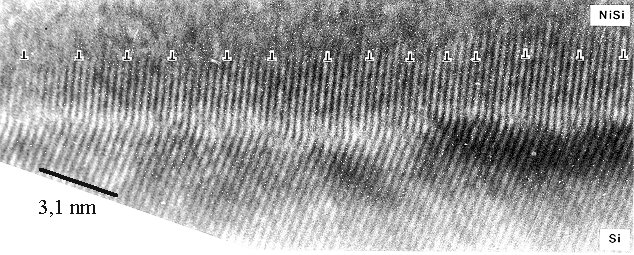
The picture below shows an extreme case of misfit dislocation for a misfit of
about 15 %. We have hexagonal NiSi with its {0001} plane in line with the {111} plane of Si.
Since both lattice planes are hexagonal in this case, we can have an epitaxial relationship between tow different Bravais
lattices. |
| |

© H. Foell |
|
|
 |
As we must expect, we have an edge dislocation (seen as ending lattice fringe) about every
7 lattice constants. This is one of the first pictures of misfit dislocations at atomic resolution. The dislocations
are so close that they could not be seen in "normal" TEM. |
© H. Föll (Semiconductor Technology - Script)
