 |
We have encountered the need for epitaxial
layers before, and we also have seen a Si
CVD process for making poly-crystalline material good enough for growing crystals. All we have to do now is to put both things together.
|
|
 |
We can use essentially the same CVD process as before, but instead of thin
rods of poly-Si which we want to grow in diameter as fast as possible, we now want to make a thin, but absolutely
perfect Si layer on top of a wafer. |
| | |
| |
 |
We now must have tremendous process control. We require:
| | |
|
 |
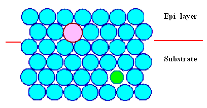
A precise continuation of the substrate lattice.
There should be no way whatsoever to identify the interface after the epitaxial layer has been deposited. This means that
no lattice defects whatsoever should be generated. |
|
|
|
 |
Doping of the epitaxial layer with high precision (e.g.
5 Wcm ± 5%), and the doping is usually very different from that of the substrate.
The picture on the right symbolizes that by the two differently colored doping atoms. |
|
|
 |
Precise thickness control, e.g. d = 1.2 µm
± 10% over the entire wafer, from wafer to wafer and from day to day. Now there is a challenge: If you met the
first point and thus can't tell where the interface is - how do you measure the thickness? (The answer: Only electronically,
e.g. by finding the position of the pn-junction produced). |
|
|
 |
Cleanliness: No contaminants diffusing into the substrate
and the epitaxial layer are allowed. | |
| |
| |
|
 |
This looks tough and it is indeed fairly difficult to make good epitaxial layers.
It is also quite expensive and is therefore avoided whenever possible (e.g. in mainstream CMOS technology). It is,
however, a must in bipolar and some other technologies and also a good example for a very demanding process with technical
solutions that are far from obvious. |
 |
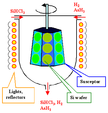
Lets look at a typical epitaxial reactor from around 1990 (newer ones tend
to be single wafer systems). It can process several wafers simultaneously and meets the above conditions. Here is a muchly simplified drawing:
|
| |
|
 |
The chemical reaction that produces the Si is fairly simple:
|
| |
| SiCl4 + 2 H2 | Þ |
Si + 4 HCl | | | (1000 oC - 1200 oC) | |
|
|
|
 |
The dopant gases just decompose or react in similar ways. However, instead of
SiCl4 you may want to use SiHxCl4–x . |
|
 |
The essential point is that the process needs high temperatures and the Si
wafer will be at high temperature! In an Epi reactor as shown above, the Si wafer surfaces (and whatever shows of
the susceptor) are the only hot surfaces of the system! |
 |
How is the process actually run? You need to meet some tight criteria for the
layer specifications, as outlined above, and that transfers to tight criteria for process control.
|
|
 |
1. Perfectly clean
Si surface before you start. This is not possible by just putting clean Si wafers inside the Epi-reactor (they
always would be covered with SiO2), but requires an in-situ cleaning step. This is done by first admitting
only H2 and Cl2 into the chamber, at a very high temperature of about 1150 oC.
Si is etched by the gas mixture - every trace of SiO2 and especially foreign atoms at the surface will be removed.
|
|
 |
2. Temperature gradients of at most (1 - 2) oC. This
is (better: was) achieved by heating with light as shown in the drawing. The high
intensity light bulbs (actually rods) consume about 150 kW electrical power (which necessitates a 30 kW motor
running the fan for air-cooling the machinery). |
|
 |
3. Extremely tightly controlled gas flows within a range of about 200
l/min H2, 5 l/min SiCl4 (or Si HCl3), and fractions of ml/min of the doping gases.
|
 |
Not to forget: Epi-reactors are potentially very dangerous machines with a lot
of "dirty" output that needs to be cleaned. All things taken together make Epi-reactors very expensive - you should
be prepared to spend several million $ if you want to enter this technology. |
|
 |
Si epitaxy thus is a process that is avoided if possible
- it costs roughly $5 per wafer, which is quite a lot. So when do we use epitaxy? |
 |
Epitaxy is definitely needed if a doping profile
is required where the resistivity in surface near regions is larger than in the bulk.
In other words, a profile like this: |
|
|
|
|
 |
By diffusion, you can always lower the resistivity and even change the doping
type, but increasing the resistivity by diffusion is not realistically possible. |
|
 |
Consider a substrate doping of 1016 cm3. Whatever resistivity
it has (around 5 - 10 Wcm), if you diffuse 2 · 1016 cm3
of a dopant into the substrate, you lowered the resistivity of the doped layer by a
factor of 2. |
|
 |
To increase the resistivity you have to compensate half
of the substrate doping by diffusing a dopant for the reverse doping type with a concentration of 5 · 1015
cm3. Not only does that call for much better precision in controlling diffusion, but you will only get that
value at a particular distance from the surface because you always have a diffusion
profile. So all you can do by diffusion is to increase the resistivity somewhat near the surface regions; but you cannot
make a sizeable layer this way. |
 |
You also may use epitaxial layers if you simply need a degree
of freedom in doping that is not achievable otherwise. |
|
 |
While DRAMs were made without epitaxy up to the 16 Mbit generation (often to
the amazement of everybody, because in the beginning of the development work epitaxy seemed to be definitely necessary),
epitaxial Si layers are now included from the 64 Mbit DRAM upwards. |
© H. Föll (Semiconductor Technology - Script)

