 |
Whenever we need SiO2 layers, but can not oxidize Si,
we turn to oxide CVD and deposit the oxide on top of the substrate - whatever it will be |
|
 |
Again, we have to find a suitable
chemical reaction between gases that only occurs at high temperature and produces SiO2. There are several
possibilities, one is |
|
|
| SiH2Cl2 + 2NO2 |
Þ |
SiO2 + 2HCl + 2N2 | | |
(900 oC) | |
|
|
|
 |
While this reaction was used until about 1985, a better reaction is offered by the
"TEOS"
process: |
| |
| Si(C2H5O)4 |
Þ |
SiO2 + 2H2O + C2H4 |
| | (720 oC) | |
|
|
|
 |
Si(C2H5O)4 has the chemical name Tetraethylorthosilicate;
abbreviated TEOS. It consists of a Si
atom with the four organic molecules bonded in the four tetrahedral directions. The biggest advantage of this process
is that it can be run at lower temperatures, but it is also less dangerous (no HCl), and it produces high quality
oxides. |
 |
Low temperature processes are important after the transistors and everything else
in the Si has been made. Every time the temperature must be raised for one of the processes needed for metallization,
the dopant atoms will move by diffusion and the doping profiles change. |
|
 |
Controlling the "temperature budget" is
becoming ever more important as junction depths are getting smaller and smaller. |
 |
CVD techniques allow to tailor some properties of the
layers deposited by modifying their chemistry. Often, an oxide that "flows" at medium temperature, i.e. evens
out the topography somewhat, is needed. Why is shown below. |
| |
|
|
 |
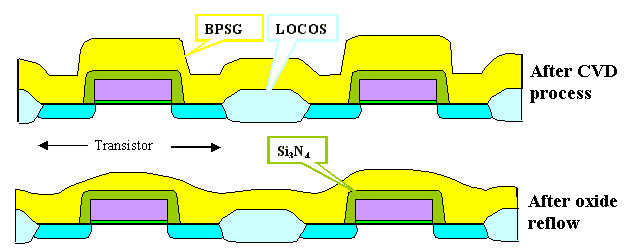
After the transistor has been made, there is a veritable mountain range. Here it is even worse
than before, because the whole "gate stack" has been encapsulated in Si3N4
- for reasons we will not discuss here. (Can you figure it out? The process is called "FOBIC",
short for "Fully Overlapping Bitline Contact"). |
|
 |
It is important for the next processes to flatten the terrain as much as possible. While this
is now done by one of the major key process complexes introduced around 1995 (in production) called "CMP" for "Chemical-mechanical polishing", before this time the key was to make
a "flow glass" by doping the SiO2 with P and/or B.
Conventional glass, of course is nothing like SiO2 containing ions like Na (which is a no-no in
chip making), but P and B are also turning quartz into glass. |
|
 |
The major difference between glass and quartz
is that glass becomes a kind of viscous liquid above the glass temperature which depends on the kind and concentration of ions incorporated. |
 |
So all you have to do during the SiO2 deposition, is to allow
some incorporation of B and/or P by adding appropriate gases. |
|
 |
As before phosphine
(PH3) is used for P, and "TMB" (=B(OCH3)3= trimethylborate)
for B. Concentrations of both elements may be in the % range (4% P and 2%
B are about typical), the resulting glass is called "BPSG" (=Bor-Phosphorous Silicate Glass). It
"flows" around 850 oC, i.e the viscosity of BPSG is then low enough to allow the surface
tension to reduce the surface areas by evening out peaks and valleys. |
|
 |
How much it "flows" can be further influenced by the atmosphere during the annealing:
O2 or even better, H2
O like in wet oxidation, enhances the viscosity and helps
to keep the thermal budget down |
|
 |
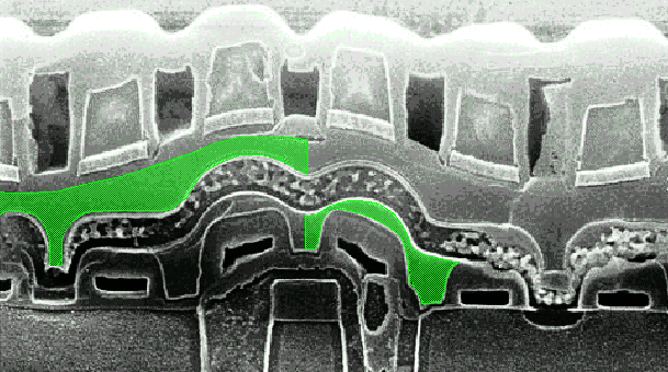
The BPSG process was a key process to VLSI (=Very
Large Scale Integration), this can be seen in any cross section of a real device. Lets look at the cross section
of the 16 Mbit DRAM
again that was shown before: |
| |
|
 |
Two layers of BPSG are partially indicated in green |
|
 |
The lower layer has been etched back to some extent; it only fills some deep
crevices in some places. |
|
 |
Both layers smoothed the topography considerably; but there can never be complete planarization
with BPSG glasses, of course. |
 |
How do we carry out an oxide CVD process? Of course, we could use a "tool" like an epi-reactor, but that would be an overkill
(especially in terms of money). |
 |
For "simple" oxide CVD, we simply use a furnace as in the thermal oxidation process and admit the process gases instead of oxygen. However,
there are certain (costly) adjustments to make: |
|
 |
CVD processes mostly need to be run at low pressure
(then often abbreviated LPCVD) - some mbar will be fine - to ensure that the
layers grow smoothly and that the gas molecules are able to penetrate into every nook and cranny (the mean free path length
must be large). The furnace tube thus must be vacuum tight and big pumps are needed to keep the pressure low. |
|
 |
We want to minimize the waste (dangerous gases not used
up) which at the same time maximizes the conversion of the (costly) gases to SiO2. But this means that
at the end of the tube the partial pressure of the process gases is lower than at the beginning (most of it has been used
up by then). To ensure the same layer thickness for the last wafer than for the first one, requires a higher temperature
at the end of the furnace tube because that leads to a higher reaction rate countering the lower gas concentration. |
|
 |
The first wafers to be exposed to the gas flow are "air-cooled" by the process gas
to some extent. We therefore need to raise the temperature a bit at the front end of the furnace. |
 |
Essentially, we must be able to run a defined temperature
gradient along the CVD furnace tube! This calls for at least three sets of heating coils which must be
independently controlled. |
|
 |
The whole thing looks like this |
| |
|
 |
Again, we see that there are many "buttons"
to adjust for a "simple" CVD oxide deposition. |
|
 |
Base pressure and temperature, flow rates of the gases, temperature profile of the furnace
with the necessary power profile (which changes if a gas flow is changed), ramping up and ramping down the temperature,
etc., - all must be right to ensure constant thickness of the deposited layer for every wafer with minimum waste of gases. |
|
 |
Changing any parameter may not only change the oxide thickness, but also its properties (most
important, maybe, its etch rate in some etching process). |
|
 |
Developing a "new" oxide CVD process thus is a lengthy undertaking, demanding
much time and ingenuity. But since this is true for every process in microelectronics, we will from now on no longer emphasize
this point. |
 |
CVD furnaces have a major disadvantage: Everything inside (including the quartz tube) is hot and
will become covered with oxide (including the wafer back sides). This is not quite so bad, because the quartz tube will
simply grow in thickness. Nevertheless, in regular intervals everything has to be cleaned
- in special equipment inside the cleanroom! Very annoying, troublesome and costly! |
 |
A "conventional" CVD furnace is, however, not the only way to
make CVD oxides. Several dedicated machines have been developed just for BPSG or other variants of oxides.
|
|
 |
One kind, adding also something new to the process, merits a short paragraph: PECVD
or "Plasma Enhanced CVD" |
| | |
|
Plasma Enhanced CVD |
| |
|
 |
As the thermal budget gets more and more constrained while more and more layers
need to be added for multi-layer metallization, we want to come down with the temperature for the oxide (or other) CVD
processes. |
|
 |
One way for doing this is to supply the necessary energy for the
chemical reaction not by heating everything evenly, but just the gas. The way to do this is to pump electrical
energy into the gas by exposing it to a suitable electrical field at high frequencies. This could induce "dielectric
losses", but more important is the direct energy transfer by collisions as soon
as the plasma stage is reached. |
|
 |
In a gas plasma, the atoms are ionized and both free electrons and ions are accelerated in
the electrical field, and thus gain energy which equilibrates by collisions. However, while the average kinetic energy and
thus the temperature of the heavy ions is hardly affected, it is quite different for the electrons: Their temperature as
a measure of their kinetic energy may attain 20.000 K. |
|
 |
(If you have problems with the concept of two distinctly
different temperatures for one material - you're doing fine. Temperature is an equilibrium property, which we do not have in the kind of plasma produced here. Still, in
an approximation, one can consider the electrons and the ions being in equilibrium with the other electrons and ions, respectively,
but not among the different species, and assign a temperature to each subgroup separately.) |
|
 |
The chemical reactions thus may occur at low nominal temperatures of just a few 100 oC. |
 |
There are many kinds of PECVD reactors, with HF frequencies from
50 kHz to >10 MHz and electrical power of several 100 W (not to be sneered at in the MHz range!). |
|
 |
Since after the first Al deposition, the temperature has to be kept below about 400
oC, (otherwise a Si - Al eutectic will form), PECVD oxide is the material of choice from now
on, rivaled to some extent by spin-on glass. |
|
 |
However, its properties are not quite as good as those of regular CVD oxide (which
in turn is inferior to thermal oxide). |
© H. Föll (Semiconductor Technology - Script)

