 |
The first integrated circuits hitting the markets in the seventies had a few 100
transistors integrated in bipolar technology. MOS circuits came several years later, even though their principle
was known and they would have been easier to make. |
|
 |
However, there were insurmountable problems with the stability
of the transistor, i.e. their threshold voltage. It
changed during operation, and this was due to problems with the gate dielectric (it contained minute amounts of alkali elements
which are some of many "IC killers", as we learned the hard way in the meantime). |
|  |
But MOS technology eventually made it, mainly because bipolar circuits need a lot of power for operation.
Even for all transistors being "off", the sum of the leakage current in bipolar transistors can be too large for many application.
|
 |
MOS is principally better in that respect, because you could, in principle, live with
only switching voltages; current per se is not needed for the operation. MOS circuits do have lower power consumption;
but they are also slower than their bipolar colleagues. Still, as integration density increased by an average 60%
per year, power consumption again became a problem. |
|
 |
If you look at the data sheet for some state of the art IC, you will encounter power dissipations
values of up to 1 - 2 Watts (before 2000)! Now (2004) its about 10 times more. If this doesn't
look like a lot, think again! |
|
 |
A chip has an area of roughly 1 cm2. A power
dissipation of 1 Watt/cm2 is a typical value for the hot plates of
an electrical range! The only difference is that we usually do not want to produce french fries with a chip, but keep it
cool, i.e. below about 80 oC. |
 |
So power consumption is a big issue in chip design. And present day chips would not exist if
the CMOS technique
would not have been implemented around the late eighties. Let's look at some figures for some more famous chips:
|
|
 |
Early Intel microprocessors had the following power rating: |
|
|
| Type | Architecture |
Year | No. transistors |
Type | Power |
| 4004 | 4bit | 1971 |
2300 | PMOS |
|
| 8086 | 16bit | 1978 |
29000 | NMOS | 1,5W/8MHz |
| 80C86 | 16bit | 1980 |
?50000? | CMOS |
250mW/30Mhz(?) | | 80386 |
16bit | 1985 | 275000 |
CMOS |
|
| | | |
| | |
| Pentium 4 | | 2004 |
| CMOS |
80 W/3 GHz |
|
|
 |
CMOS seems to carry the day - so what is CMOS technology? |
| | |
|
CMOS - the Solution |
| |
|
 |
Lets first see what "NMOS" and PMOS" means. The
first letter simply refers to the kind of carrier that carries current flow between source an drain as soon as the threshold
voltage is surpassed: |
|
 |
PMOS stands for transistors where positively
charged carriers flow, i.e. holes. This implies that source and gate must be p-doped
areas in an n-doped substrate because current flow begins as soon as inversion
sets in, i.e. the n-type Si between source and drain is inverted to Si with holes as the majority carriers |
|
 |
NMOS then stands for transistors where negatively charged
carriers flow. i.e. electrons. We have n-doped source and drain regions in a p-doped substrate. |
 |
The characteristics, i.e. the source-drain-current vs. the gate voltage, are roughly symmetrical
with respect to the sign of the voltage: |
| |
|
|
 |
The red curve may stand for a NMOS or n-channel transistor, the blue one then
would be the symmetrical PMOS or p-channel transistors. The threshold voltages are not fully symmetric if
the same gate electrode is used because it depends on the difference of the Fermi energies of the gate electrode materials
and the doped Si, which is different in the two cases. |
|
 |
Anyway, for a given gate voltage which is larger than either threshold voltage applied to the
transistor, one transistor would be surely "on", the other one "off". |
 |
So if you always have a NMOS and a PMOS transistor in series, there will never be any static current flow; we have a small dynamic current component only while switching
takes place. |
| |
| |
|
 |
Can you make the necessary logical circuits this way? |
| |
 |
Yes you can - at least to a large extent. The illustration shows an inverter
- and with inverters you can create almost anything! |
| |
 |
Depending on the right polarities, the blue PMOS transistor will be closed if there is a gate voltage
- the output then is zero. For gate voltage zero, the green NMOS transistor will be closed, the PMOS transistor
is open - the output will be VDD (the universal abbreviation for the supply voltage). |
| |
 |
So now we have to make two kinds of transistors- NMOS
and PMOS - which needs substrates with different kind of doping - in one integrated
circuit. But such substrates do not exist; a Silicon wafer, being cut out of an homogeneous crystal, has always one doping kind and level. |
|
 |
How do we produce differently doped areas in an uniform substrate? We remember what we did
in the bipolar case and "simply" add another diffusion that converts part of the substrate into the different
doping kind. We will have to diffuse the right amount of the compensating atom rather deep into the wafer, the resulting
structure is called a p- or n-well, depending on what kind of doping you get.
|
|
 |
If we have a p-type substrate, we will have to make a n-well.
The n-well then will contain the PMOS transistors, the original substrate the NMOS transistors. The
whole thing looks something like this: |
| |
|
 |
By now, even the "simple" MOS technology starts to look complicated. But it
will get even more complicated as soon as you try to put a metallization on top. The gate structure already produced some
"roughness", and this roughness will increase as you pile other layers on top. |
|  |
Let's look at some specific metallization problems (they are also occurring in bipolar technology,
but since you start with a more even surface, it is somewhat easier to make connections). |
|  |
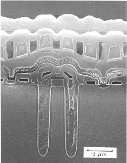
A cross-section through an early 16
Mbit
DRAM
(DRAM=Dynamic Random Access Memory; the work horse memory in your computer) from
around 1991 shown below illustrates the problem: The surface becomes exceedingly wavy. (For enlarged
views and some explanation of what you see, click on the image or the link) |
 |
Adding more metallization layers becomes nearly impossible. Some examples of the difficulties
encountered are: |
|
 |
1. With wavy interfaces, the thickness between two layers varies considerably, and, since making
connection between layers need so-called "via"
holes, the depths of those vias must vary, too. This is not easily done! And if you
make all vias the same (maximum) depth, you will etch deeply into the lower layer at places where the interlayer distances
happens to be small. |
|
 |
2. It is very difficult to deposit a layer of anything with constant thickness
on a wavy surface. |
|
 |
3. It is exceedingly difficult to fill in the space between Al lines with some dielectric
without generating even more waviness. The problem then gets worse with an increasing number of metallization layers. |
 |
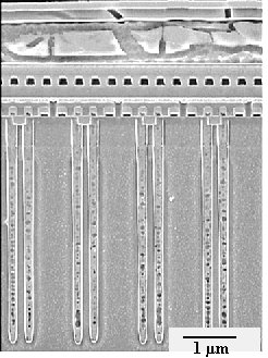
The
64 Mbit DRAM, in contrast, is very flat. A big break-through in wafer processing around 1990 called "Chemical mechanical Polishing" or CMP allowed to planarize wavy
surfaces. |
| |

Cross section 16 Mbit DRAM (Siemens) |

Cross section 64 Mbit DRAM (Siemens) |
|
 |
It's time for an exercise: |
| |
|
| | |
© H. Föll (Semiconductor Technology - Script)