 |
There seems to be no problem. The transistors are insulated from
each other because one of the pn-junctions between them will always be blocking. However:
We must also consider "parasitic transistors" not
intentionally included in our design! |
|
|
| |
|  |
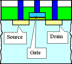
If in the space between transistors a wire is crossing on top of the insulating layer as shown
in the illustration, it will, on occasion be at high potential. The drain of the left transistor together with the source
of the right transistor will now form a parasitic transistor with the insulating layer
as the gate dielectric, and the overhead wire as the gate electrode. |
|
|
 |
Everything being small, the threshold voltage may be reached and we have a current path where there should
be none. |
| |
 |
This is not an academic problem, but a typical effect in integrated
circuit technology, which is not found in discrete circuits: Besides the element you
want to make, you may produce all kinds of unwanted elements, too: parasitic transistors, capacitors, diodes, and even thyristors. |
| | | |
|
 |
How we produce the additional insulator called field
oxide between the transistors will concern us later; here it serves to illustrate two points: |
|  |
Insulation is not just tricky for bipolar transistors, it is a complicated business with MOS
technology, too |
|
 |
There is now some "topology" - the interfaces and surfaces are no longer
flat. Looks trivial, but constitutes one of the major problems of large-scale integration! |
 |
Note that the gate - substrate part of a MOS transistor is, in principle, a capacitor. So we can now make capacitors, too. |
|
 |
However, if we need a large capacitance - say some 50 fF (femto
Farad) - we need a large area (several µm2) because we cannot
make the dielectric arbitrarily thin - we would encounter tunneling effects, early breakdown, or other problems. So we have
to have at least a thickness of around 5 nm of SiO2. If the capacitor area than gets too large,
the escape road is the third dimension: You fold the capacitor! Either into the substrate,
or up into the layers on top of the Si. |
|
 |
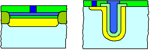
The "simple" way of folding integrated capacitors into the substrate is shown
in the right hand side of the next illustration |
| |

| | Planar capacitor | "Trench" capacitor |
|
 |
The planar capacitor (on the left) and the "trench"
capacitor (on the right) have a doped region in the Si for the second electrode, which must have its own connection
- in the drawing it is only shown for the trench capacitor. We learn two things from that: |
|  |
1. Large scale integration has long since become three-dimensional - it is no longer
a "planar technology" as it was called for some time. This is not only true for truly three-dimensional elements
like the trench capacitor, but also because the processes tend to make the interfaces rough as we have seen already in the case of the field oxide.
|
|
 |
2.
The names for certain features generally accepted in the field, are on occasion simply wrong! The capacitor shown above is not folded into a trench (which is something deep and long in one lateral direction, and small in the other direction),
but into a hole (deep and small in both lateral directions). Still, everybody calls
it a trench capacitor. |
 |
The key processes for ICs more complex than, say, a 64 Mbit memory, are indeed
the processes that make the surface of a chip halfway flat again after some process has been carried out. |
 |
Again, there is a special message in this subchapter: Integrating MOS transistors, although
supposedly simpler than bipolar transistors (you don't need all those pn-junctions), is far from being simple or
obvious. It is again intricately linked to specific combinations of materials and
processes and needs lots of ingenuity, too. |
|
 |
But we are still not done in trying to just get a very coarse overview of what integration
means. If you take an arbitrary chip of a recent electronic product, changes are that you are looking at a CMOS chip, a chip made with the "Complementary Metal Oxide Semiconductor"
technology. |
|
 |
So lets see what that implies. |
© H. Föll (Semiconductor Technology - Script)
