 |
This will be a short statement of very elementary facts from basic physics or
electrical engineering. |
|
 |
Any "wire" used to carry electricity has a resistance
R (we will not consider superconductors here) - just measure it via R = U/I. Its
resistance measured in Ohms (O) might be small, but it is never zero. |
|
 |
Any "wire" that serves its purpose is isolated
from the environment by some dielectric (air or some insulation material) having some dielectric constant er |
|
 |
At some distance from any wire is always another conductor
at some arbitrary potential. Even if our hypothetical device consist of a wire only, there is always the "earth"
somewhere at (by definition) zero potential. It follows: Any wire has some capacitance
C to something else. Again, this unintentional parasitic capacity
might be small, but it is never zero. Moreover, whatever value it has, it is proportional to the dielectric constant er of the dielectric in question. |
 |
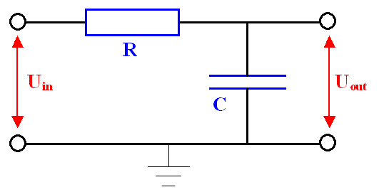
Any wire (at not too high frequencies) thus can be described
by an equivalent circuit diagram that looks like this. |
| |
|
 |
What happens if we put a digital signal on one end of the wire, which we call the "input"
end? Ideally, that means that the voltage or better potential on the wire (the not grounded upper "wire" in the
picture above) jumps from 0V to, say, 5V instantaneously. What happens at the output? |
|  |
Ideally, the potential would also go up suddenly after a certain time t0
which is dictated by the speed of light c, because nothing can move faster than that. we thus have t0
= l/c with l = length of the wire, and c = speed of light "in" the
wire, whatever that means. |
|
 |
However, as soon as we raise the potential at the input, we have to put charge in the parasitic
capacitor C. The voltage at this capacitor is the output voltage, and for a voltage U we need
to have the charge Q = C · U stored in the capacitor. |
|  |
For that a current has to flow into the capacitor, and that current will be restricted by
the resistance R. Note that for just transmitting information as jumps in the potential, current flow would
not really be necessary, but our parasitic capacitor needs charges flowing in (and later out) of it, if its potential is
to change. |
 |
It is easy to describe quantitatively what happens. For the current I flowing
during the charging of the capacitor we have two equations. |
|
|
| I = C · |
dUout
dt |
= |
Uin – Uout
R |
|
|
|
 |
This is an easy differential equation. We will just look at the solutions for the two cases
of Uin going "up" to Uin-on at t = 0 and at Uin
going "down from " to Uin-on to 0; again at t = 0. |
|
 |
For the "going up" case we obtain |
|
|
|
Uout = Uin-on · {1 – exp– (t/RC)} |
|
|
|
 |
This describes an output voltage that increases as a function of time with the time constant
RC; i.e. after the time RC the output voltage is Uout = Uin-on
· (1 – 1/e) = 0.63 · Uin. |
 |
If we look at what happens if the input voltage is "going down", i.e.switched to
zero (after it has been on long enough to make sure the output voltage is equal to the input voltage), we obtain in the
same way: |
| |
|
Uout = Uin-on · exp– (t/RC)} |
|
|
|
 |
The output voltage thus decays with the time constant RC from the "on"
value to zero. |
 |
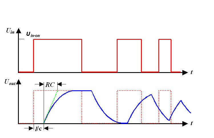
Putting all of this together for some input signals gives the following picture: |
| |
|
 |
What we have now is that at the output end of a "wire" with length l,
the voltage will start to go up after a time t0 = l/c with c = speed of light, i.e.
the speed of electromagnetic wave propagation in the wire (c might not be exactly the speed of light in vacuum, but
that is not the important part here). |
|
 |
The voltage then will start to increase, after the time constant
RC it will be at about 2/3
of the input voltage. After a few time constant it is identical to the input voltage. |
|  |
If the input signal goes "down" again, the output signal will follow, again with
a delay of t0 and then with a decay time again given by the time constant RC. |
 |
Now consider that we are discussing digital applications. The output voltage will be interpreted
as either "0" or "1"; let's say the low potential = 0, the high potential = 1. |
|
 |
During the transients of the voltage, we are neither here nor there, but our electronic circuitry
typically will interpret a potential < U/2 as 0, > U/2 as 1. That simply
means that the time it takes for a signal to travel through a wire with the length l and then to be recognized
by what ever follows as a "1" is t0 plus about one time constant RC
of the wire. That means we have an additional delay time given by the "undesirable" properties of the wire. |
|
 |
Even worth! The picture makes clear, that as soon as you start to transmit signals shorter
than a few time constant RC, your output signal can't even follow the input any more. In other words, at input
frequencies much larger than about 1/RC, you run into big problems. |
 |
In plain words: You cannot run your circuitry at frequencies > 1/RC - give
or take a factor of 2 - 3.! |
 |
Where does that leave us? How large is RC typically for the "wires"
in an integrated circuit. Let's look at a simplified situation: |
|
|
|
 |
Let's look at a typical Al or Cu conductor on a chip with a length of 1 cm,
a cross-sectional area of 0.5 µm2 and the specific resistivity of a
typical metal of about
2 mWcm. The total resistance of our "wire" then is |
| |
| R = |
r · l
A |
= |
2 · 10–6 Wcm2
0.5 · 10 –8cm2 |
= 400 W |
|
|
|
 |
The capacitor in the picture is formed by the two longish "plates", each with an
area l · w = l · A/dOx (w is the lateral extension
of the conductor strip; i.e w = A/dOx). With typical numbers like dOx
= 300 nm, dielectric constant e = 3.7 (the value for SiO2), the
capacity of the wires then is |
| |
| C = ee0 |
A · l
d2Ox | = |
3.7 · 8.85 10–12 A · s · 0.5 · 10–12
m2 · 10–2 m
9 · 104 · 10–18 V ·
m · m2 | = 1.82 · 10–12 |
A · s
V |
= 1.82 pF |
|
|
 |
For our time constant RC we obtain |
|
|
| R · C = 400 · 1.82 · 10–12
| A · s · V
V · A |
= 7.28 · 10–10 s |
|
|
 |
The maximal frequency we can transmit through this "wire " then would be nmax = 1/RC = 1.36 GHz. This may appear a bit "handwaving" or just
a rough estimation; nevertheless, the problem should be clear. |
|
 |
On a real chip, signals travel through many wires; possibly far shorter then 1 cm, and possibly
not all the way atop another wire, so the capacity could be somewhat smaller. On the other hand, on a real chip, theer are
also neighboring wires to the left and the rigth, which increases the capacity. |
|
 |
Nowadys, we always use a multilevel metalization scheme and being smart, we will keep the small wires
on the lower levels quite short, and give the long wires (i.e. for power supply) on the upper levels a large cross-section
- keeping R down in both cases. Nevertheless, a clock frequency of 4 GHz, standard nowadays on many
mass-produced microprocessors, is an amazing feat considering the number from above. |
|
 |
Essentially, the specific resistivity r of the conductor
and the dielectric constant e of the "intermetal
dielectric" limit the maximal frequency of the chip after all tricks of an optimized geometry have been exhausted. |
 |
Decreasing r by a factor of about 1.6 by switching
from Al to Cu started to make a lot of sense around the year 2000. |
|  |
Replacing the ubiquitous SiO2 with an e » 3.7
by a so-called "low k" dielectric with an e
of 1.5 or so would make a lot of sense right now (2005), unfortunately, nobody knows exactly how to do it
(despite a Billion $ or so, that have been spent on the search for a low-k material up to now). |
| | |
© H. Föll (Semiconductor Technology - Script)


![]() 5.1.3 Basic Concepts of Connecting Transistors
5.1.3 Basic Concepts of Connecting Transistors ![]() 5.1.4 Integrated MOS Transistors
5.1.4 Integrated MOS Transistors ![]() 5.1.5 Integrated CMOS Technology
5.1.5 Integrated CMOS Technology