Cross Section of 16 Mbit DRAM and 64 Mbit DRAM
 |
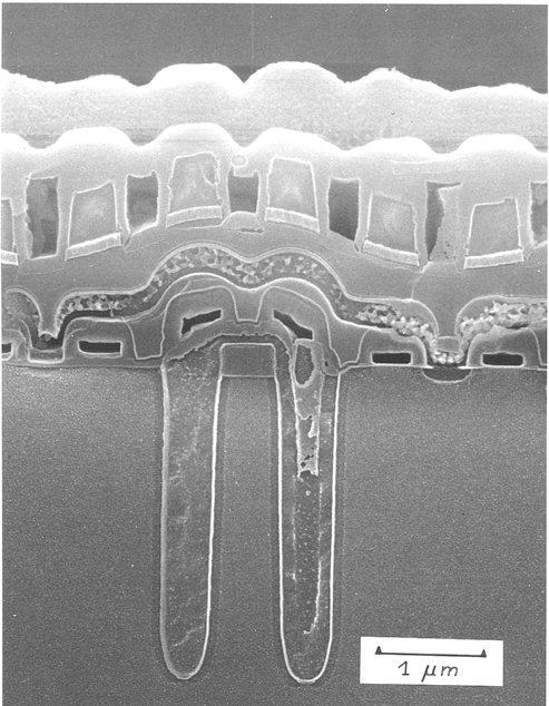
Below a large SEM micrograph showing the cross-section of an (early) 16
Mbit DRAM. |
| |
|
|
 |
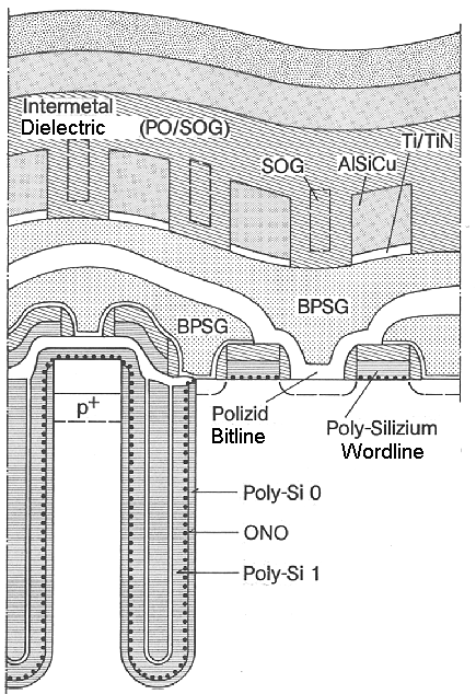
Some explanations:
- The two deep "trenches" (they are really
holes) contain the capacitors. There dielectric (with ca. 7 nm far too thin to be visible) is "ONO",
a triple layer of Oxide - Nitride - Oxide.
- The trench os lined with poly-Si as a first electrode and as the second electrode.
- To the left and right two transistor gates are visible. The sources of both transistors is the (poly-Si) electrode
lining the trench and the diffused areas being contacted by the "Polizid bitline". "Polizid" means a
double layer of poly-Si and MoSi2 Molybdenum-silicide.
- The "poly-Si wordline" runs perpendicular to the picture and connects the gates of the transistors
- The "BPSG" layers denote SiO2 doped with B and P that serves as insulating
dielectric. It is essentially a glass.
- Parallel to the word lines are Ti/TiN/AlSiCu lines. They contact the wordlines every once in a while to decrease
the ohmic resistance. The consist of a layer sequence: Ti, TiN, and Al doped with about 0,5%
of Si and Cu.
- On top of this first metal layer is another one running across the picture.
- The metals are insulated by the intermetal dielectric composed of plasma-oxide (PO) that contains spin-on-glass
(SOG) in the interstices.
|
 |
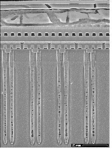
Below the successor of the 16 Mbit DRAM, the 64 Mbit DRAM from a development
stage around about 1996. |
| |
|
|
 |
The structure is essentially the same, but all layers have been planarized. |
| | |
 With frame

 6.3.1 Physical Processes for Layer Deposition
 5.1.5 Integrated CMOS Technology
 6.2.3 CVD for Poly-Silicon, Silicon Nitride and Miscellaneous Materials
 6.5.2 Resist and Steppers
 Poly-Silicon
© H. Föll (Semiconductor Technology - Script)


