 |
We know that we need III-V semiconductors for optoelectronic
products, so we have to make single crystals as input to our optoelectronics factory. |
|
 |
We may use those single crystal for the product or we may just use them as the
substrate for the thin film that will contain the product. Whatever - they better be as perfect as possible because any
defect present at the surface (e.g. a dislocation ending a the surface) will simply continue in any epitaxial
layer we might produce. |
|
 |
Let's look at GaAs single crystal production as en example for other III-V's
like InP or GaP. However, not all III-V's can be grown on a similar way; we will come to that.
|
 |
The Czochralski
method for growing crystals should work for GaAs, too. So let's try it and see why it is far more difficult to
grow compound single crystals than Si (or Ge) single crystals |
| | |
| |
|
 |
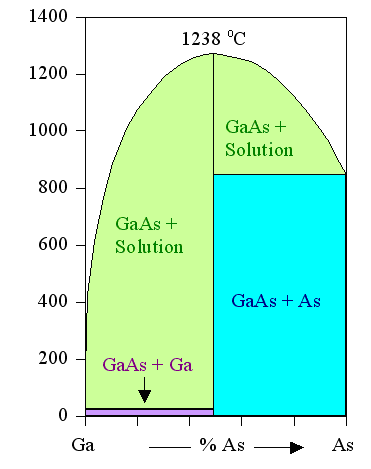
The melting point of GaAs, however, is Tm(GaAs)=1.238
oC. This is a first indication that things might not be quite as simple as they look. Obviously, we
now need a phase diagram of the Ga - As system. Here it is: We mix Ga and As in a (molar) ratio
of 50:50 and melt it in a crucible. That should be easy, because both elements have low melting points (Ga:
30 oC; As: ? oC - it actually doesn't melt but evaporates at a sublimation or
boiling point of 615 oC). | |
|
|
 |
So what happens if our mixture is not 50 : 50 but 49.999 : 50.001? We will have
little droplets of liquid in our growing crystal, that solidify later and probably cause defects at a concentration that
is large - in comparison to what we call "low defect concentration". |
|
|
 |
To make things worse, whatever you mix together and melt, at the required 1.238 oC
the As in the melt will evaporate off quickly; the concentration thus changes as a function of time. |
|
 |
The catchword now is "liquid
encapsulation technique" (LEC). |
|
|
 |
The melt in the crucible will be enclosed in B2O3, a viscous
liquid at the growth temperature. It encloses the entire melt, i.e. sits between crucible and melt and on the surface. Obviously,
we have another case of getting surface energies right here.
The seed crystal is now dipped through that layer into the melt - and so on. |
|
|
 |
There is no way that the crystal you get will come close in quality to Si crystals.
The present state of the art is given in this relatively short
article given at that Czochralski-Symposium 2003 in Poland |
|
|
 |
You will not understand some of the topics in the article, but you will get a feeling for
the complexity involved in growing good GaAs single crystals. |
|
|
| |
|
 |
Of course, any other III-V compound crystals grown in a similar way runs
into all the difficulties hinted at above plus some of its own. This is particularly true for GaN, which will be
shortly discussed below. |
 |
Less of course, there are some other ways of growing GaAs (and other) single
crystals but we cam't go for that here. |
| |
| |
| |
|
Gallium Nitride
|
| |
| |
|
 |
In the (slightly changed) words of Dr. Yoke Khin Yap;
Department of Physics, Michigan Technological University: | |
|
|
| |
|
|
 |
High-quality GaN single-crystals are still not possible because the melt
growth of GaN single-crystal is prohibited due to the extremely high decomposition pressure (~ 45000 atm)
involved at the melting point (~2500 °C). At present, GaN single-crystals can be grown by the solution
method at (1300 - 1600) °C and N2 gas pressure of (10000 - 17000) atm. Because of the
need of high temperatures and gas pressures, the solution growth method is not suitable for mass-production of GaN
single-crystals. | |
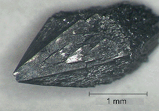
Single
crystal of GaN |
From Yap Research Lab, Michigan Tech |
|
 |
We have been growing high-quality GaN single-crystals by a Na flux method at
800 °C and <50 atm. This technique is promising for mass production of GaN single-crystals
at significantly low temperatures and pressures. A similar approach is also applicable for growing other nitride crystals
like w-AlN and h-BN. | |
| |
| |
|
 |
So how come we have a flourishing GaN industry, making UV - blue
LED's and Lasers? |
|
 |
Because the input to a "commercial" GaN factory consists of substrates
with a thin GaN layer on it. The substrate is either Al2O2 with a lattice misfit of 13.8% and a thermal expansion coefficient mismatch of 25.5% |
|
 |
Not good. So you look for a better substrate and find SiC. Not so hot either,
look at our "master graph".
Any you now need SiC single crystal (see below). |
 |
Nevertheless, GaN made it into the ranks of serous semiconductors with
billion € or so business attached. What we learn form this is that semiconductor technology, like politics,
is the art of the possible ("Politik ist die Kunst des Möglichen; Otto von Bismarck) |
| |
|
 |
In most cases, large single crystals are grown from a melt or some solution (e.g.
quartz, or sugar if you leave you coffee cup around too long), but this is not a feasible option for SiC single crystal
growth since SiC does not have a liquid phase under normal conditions (i.e. without applying a large pressure). SiC
is also extremely hard (close to diamond) and therefore has a high melting point (or is it the other way around?). |
|
 |
There is also, in principle, no crucible material that could contain molten SiC
at is nominal melting point temperature of < 2.500 oC. Nevertheless, SiC was grown from a melt
at 2200 oC and 150 bar in a recent study, but this is probably not a commercially viable process. |
 |
We need a basically new method of crystal growth, and the main method used nowadays
is physical vapor transport (PVT) also known as seeded sublimation growth or modified Lely method. |
|
 |
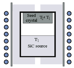
A piece of SiC is heated to (1800-2600) oC at low pressure. Due to
the high sublimation rate, SiC vapor forms and deposits itself on a cooler single-crystalline seed crystal. Straightforward
and basically simple, as shown in the schematic picture below. |
 |
However, pondering the situation, some questions should come to mind: |
|
 |
What materials can you use for the crucible and everything else that gets hot? After all,
not many materials can cope with temperatures above 2000 oC! Well, you are basically stuck with graphite,
and maybe a bit of Ta here and there. That means, of course, that you are forming SiC also on your crucible
walls and everywhere else. If it flakes off, you will have a defect problem. |
|
 |
What kind of growth rate can you get? As you would expect:
Not much! Growth rates depend on many parameters, but are in the range of 0.2 - 2 mm/hr. That's about a factor of
50 slower than the growth rates for Si crystal pulling and that makes SiC crystal growing automatically
expensive |
|
 |
What polytype will you get (hoping that it will not be
a mixture)? What determines what you get? Can you control it and, if yes, how? |
|
 |
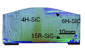
Good questions! First, you might get mixtures as shown in the picture (courtesy
of the Erlangen group). Otherwise, the following parameters are essential:
- Polytype of the seed crystal (as you might have guessed).
- "Face" of the seed crystal; i.e if the surface is a C- or a Si layer. If you start with a 4H-SiC
seed crystal, for example, you tend to get 4H-SiC if you have a C-face, and 6H-SiC if you have a Si
face. Why? Nobody really knows.
- Temperature difference and - gradient betwen SiC source and seed. Small values tend to favor 4H-SiC, larger
values 6H-SiC growth.
- Gas composition. Whatever gas you add will influence the polytype you obtain. C-rich gases, for example, promote
4H-SiC growth
- The pressure, oddly enough, seems not to have a large influence on polytypie.
Note that while the polytype 6H is the easiest to grow, 4H would be favored by the power electronics
industry. |
 |
Last not least: What kind of crystal quality do you get? What is the dislocation
density? |
|
 |
The bad news is: the dislocation density is high. The good news is, you do not worry too much
about that - you worry about something weird called "micropipe (and mixtures
of polytypes, and all kinds of stacking faults or special boundary faults, and carbon inclusion, or Si inclusion,
or big voids, ...). |
|
 |
What are micropipes? Well, micropipes are hollow channels running through
the lattice; the diameter of these pipes is (0.1 - 5) µm. One might consider them to be screw dislocations with
a gigantic Burgers vector and a hollow core. |
|
 |
Micropipes also will definitely kill any device that contains one of them. They thus must
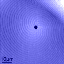
be avoided as much as possible! Micropipes are also somehow connected to the growth mechanism of the crystal. This is neatly
illustrated in the picture on the right (taken with a scanning force microscope, courtesy of H. Strunk; Uni Erlangen) where typical growth spirals are visibly centered around a micropipe. |
| |
 |
 |
| | SiC crystal growth reactor (simplified!) |
SiCsingle crystal - cross section |
Micropipe with growth spirals |
|
 |
Let's look at the state of the art of what is around. To quote from the product
sheet of the major SiC supplier Cree, Inc. (located somewhat ironically in Silicon Drive 4600 in Durham, North-Carolina,
USA): |
|
 |
At present, wafer diameters are 50.8 mm or 76.2 mm; doping (usually
with N for n-type and Al for p-type) at high levels produces resistivities in the 0.0x mWcm region. Or there is no doping for semi-insulating stuff. 4H- and 6H-SiC polytypes
are sold |
 |
The 2003 state of the art (mostly in the laboratories and not necessarily
on the market) is summarized in the following table: |
|
|
| Diameter | 100 mm
"Four-inch" |
For Si, 100 mm was the standard back in the late 70ties/early 80ties). |
| Defects | Micropipes |
< 1 cm–2for 3''
< 30 cm–2for 100 mm |
Increasing wafer size usually dramatically increases micropipe density | | Dislocations |
3 · 103cm–2 achieved |
Factor 10 reduction |
|
|
Of course, in the many laboratories (university and industrial) devoted to SiC,
some data might be even better. |
|
|
|
The Rest |
| |
|
 |
Just kidding. All we can do here is to look at a list of what is left over |
 |
Germanium. |
|
 |
Obviously, Ge wafer technology can follow the Si lead in principle.
It should be even somewhat easier to grow Ge single crystals because the melting point of Ge is lower (938
oC vs. 1410 oC, resp.) |
|
 |
However, while there is a lot of SiO2 around to start from, where do you
find Ge-minerals? Indeed, the price of germane,GeH4, needed for starting, is orders of magnitudes
higher that that of silane, SiH4. |
|
 |
All things considered, you can get pretty good dislocation free Ge wafers - up to one
or two 300 mm diameters - but for a price. The total quality, however, is not as good as the mass-produced 300
mm Si wafer. |
 |
II-VI Semiconductors |
|
 |
There are many kinds, and you may have to find a specific way of growing single crystals for
each kind. |
|
 |
The state of the art in terms of what you can buy are small and rather imperfect single crystals
of CdSe, ZnO and ..... |
 |
Everything else mentioned in chapter
2. |
|
 |
Forget it .No single crystals to speak of - yet. |
 |
Special Wafers |
|
 |
Some Si microelectronic factories have switched from regular Si wafers as input
to "SOI"
wafers; "Silicon on Insulator"; e.g. AMD in Dresden |
|
 |
Read the article
in the link if you want to find out what SOI is all about |
© H. Föll (Semiconductor Technology - Script)
