| Critical Technology to
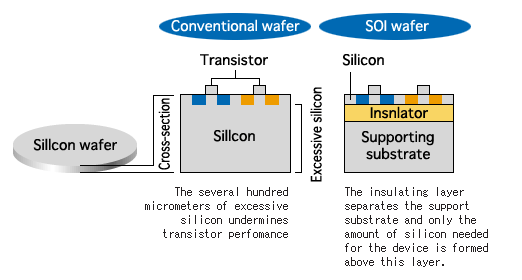
Support Development & Production of Next-Generation Semiconductors LSIs undergo rapidly developing technological innovations and are always expected to provide higher processing speeds with lower power consumption. The Silicon-On-Insulator ( SOI ) wafer is drawing attention throughout the industry as a high-potential next-generation wafer. The silicon wafers found in existing semiconductor devices usually have a thickness of several hundred microns. However, the electrically active domain of a wafer is limited to its surface, in fact, less than a few microns of thickness is needed. The remained part of a wafer is used as substrate. Unfortunately, this excess material causes both a rise in power consumption and a fall in the operating speed of the device. The SOI wafers incorporate an insulating layer between its very thin ( less than a few microns) active domain and its much thicker substrate. The substrate is isolated and can thus no longer deteriorate the speed or efficiency of the active layer. In short, the SOI wafer's technological breakthrough accelerated speeds with reduced power consumption. |
|
 |
|
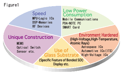
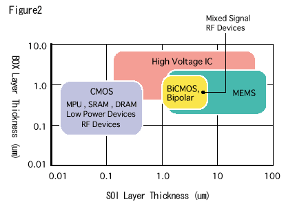
| SOI' s Advantage As the SOI devices have features operating stably at high temperature, under cosmic rays and radiant ray, the SOIs have come into practical use in aerospace field. And now, the end of LSIs' development coming, the SOIs are expected to be a breakthrough technology together with Cupper and Low-K dielectric. The SOI wafer is not only faster and more energy efficient than conventional silicon wafers, it also has higher device packing densities. For the demand of faster speed, MPUs have been developed by SOI technology for commercial use. And, these properties make it ideal for use in note-type personal computers, portable computer terminals, and microwave communications ICs like those found in cellular phone. In addition, the SOI wafers are expected to use for MEMS applications taking advantage of its unique construction. We suggest the use of the SOI according to its features in Figure 1. And, we give examples of SOI's layer configuration depending on semiconductor devices in Figure 2. |
|
 |
|
 |
|
| Copyright (c) CANON INC. |
|