 |
There is no such thing as plain SiC! |
|
 |
Instead, whenever you look in the literature, you will find names like 3C-SiC,
6H-SiC, 4H-SiC, or 2H-SiC. In other words: There are many different polytypes
of SiC. |
|
 |
Polytypism is a special case of Polymorphism,
which means that a given element or compound can assume more than one crystal structure. Polytypism simply is the one-dimensional
variant of polymorphism. |
 |
SiC (unfortunately) is sort of the paradigmatic material for polytypism.
The always identical hexagonal two-dimensional SiC layers can form many crystal structures by different ways of stacking
the layers on top of each other - that's why it is one-dimensional. See "MatWiss
I" (in German) for the basics of how crystals can be formed by stacking atomic layers. |
|
 |
SiC does not just have a few polytypes, it has more than 200! Now
you have a problem: which one is the best for the application you have in mind, and if you know that, can you actually make
it all by itself (and not in a mix with all the others)? |
|
 |
SiC is also the only stable group IV - IV
compound semiconductor. No other combination of the elements C, Si, Ge,
Sn exists in a defined lattice (and not just as mixed crystal like Si-Ge). |
|
 |
All polytypes have a rather large
indirect bandgap and other properties, which make SiC a very interesting material for many applications. |
|
 |
As you may have guessed, SiC is devilishly difficult to grow as a (large)
single crystal of one polytype with low defect density. SiC actually boasts a
particular (and very bad) lattice defect all of its own - so-called micropipes - the likes of which have not (yet) been found in other crystals.
|
 |
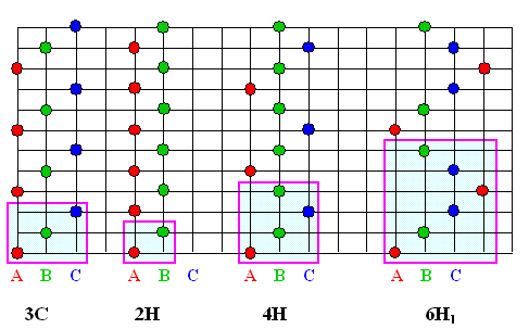
The formal way of identifying polytypes, ie.e. the nomenclature
of the polytypes, is explained in the link (basic module); here we just look at the more important variants in terms
of the familiar "ABC" stacking definition.
The basic building block (not necessarily a unit cell) is highlighted in light blue. |
| |
|
|
 |
Upon contemplation, you should be able to notice that the "3C"
structure is nothing but the ABC stacking sequence of a close-packed fcc lattice; the 2H is the corresponding
simple hcp structure resulting from an AB stacking sequence. |
|
 |
Your guess then that C stands for "cubic"; H for hexagonal,
is correct. If an "R" comes up in variants not shown here, it stands for rhombohedral. |
|
 |
In some older nomenclature, cubic SiC is also known as b-SiC;
the hexagonal phase (6H-SiC more or less) is the a-SiC |
 |
Not only the structure of SiC polytypes is different, but so are their
electronic properties. |
|
 |
The always indirect
band gap varies from 2.4 eV for the cubic 3C-SiC to 3,3 eV for the simple hexagonal 2H-SiC
variant. Other relevant parameters like carrier mobility might be quite different, too. Some values (mostly adpated from
the publications or presentations of Erlangen (Germany) SiC group) are shown below |
| |
| | 4H-SiC | 6H-SiC | 15R-SiC | 3C-SiC |
| Band Gap [eV] | 3.265 | 3.023
3.03 | 2.986 | 2.390 |
| Lattice Constant [Å] | a | 3.08
3.073 | 3.08 | 3.08 |
4.36 | | c | 10.05 | 15.12 | 37.70 | - |
| Effective Mass [mc] |
me | 0.37 | 0.69 | 0.53 - 0.28 | 0.68 - 0.25 |
| mh | 0.94 | 0.92 | - | - |
| Mobility (@ 300K) [cm2/Vs] | µe | 500 | 300 |
400 | 900 | | µh | 50 | 50 | - | 20 |
Thermal conductivity (RT)
[W/cm · K] | 3.0 - 3.8 | 3.0 - 3.8 |
| |
|
|
 |
If you look at the table long enough, you should now actually
have a question! |
 |
Anyway, besides the rather large bandgap, the effective masses and the mobilities
are not so remarkable compared to the more standard semiconductors. |
|
 |
However, if you compare on a more specific
level, there are definite advantages. Activate the link if you are interested. |
| | |
|
Crystal Growth, Wafers and Defects |
| | |
 |
Here we will only look at the basics; details are left to an advanced module. |
 |
In most cases, large single rystals are grown from a melt (e.g. Silicon) or some solution (e.g. quartz, or sugar if you leave you
coffee cup around too long), but this is not a feasible option for SiC single crystal growth since SiC does
not have a liquid phase under normal conditions (i.e. without applying a large pressure). SiC is also extremely hard
(close to diamond) and therefore has a high melting point (or is it the other way around?). |
|
 |
There is also, in principle, no crucible material that could contain molten SiC
at is nominal melting point temperature of < 2.500 o C. Nevertheless, SiC was grown from a melt
at 2200 oC and 150 bar in a recent study, but this is probably not a commercially viable process. |
 |
We need a basically new method of crystal growth. Some "older" techniques
are described in the link, the main method used nowadays is physical vapor transport (PVT) also known as seeded
sublimation growth or modified Lely method. |
|
 |
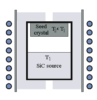
A piece of SiC is heated to (1800-2600) o C at low pressure.
Due to the high sublimation rate, SiC vapor forms and deposits itself on a cooler single-crystalline seed crystal. |
|
|
|
 |
Straightforward and basically simple, as shown in the schematic picture on the right. |
|
 |
However, pondering the situation, some questions should come to mind: |
|
 |
What materials can you use for the crucible and everything else that gets hot?
After all, not many materials can cope with temperatures above 2000 oC! |
|
|
 |
Well, you are basically stuck with graphite, and maybe a bit of Ta here and there.
That means, of course, that you are forming SiC also on your crucible walls and everywhere else. If it flakes off,
you will have a defect problem. | |
 |
What kind of growth rate can your get?
| |
|
 |
Well, as you would expect: Not much! Growth rates depend on many parameters, but are in the
range of 0.2 - 2 mm/hr. That's about a factor of 50 slower than the growth rates for Si crystal pulling
and that makes SiC crystal growing automatically expensive |
|
 |
What polytype will you get (hoping that it
will not be a mixture)? What determines what you get? Can you control it and, if yes, how? |
|
|
| |
| |
|
 |
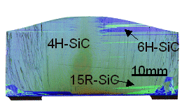
Good question! First, you might get mixtures as shown in the picture (courtesy of the Erlangen
group). Otherwise, the following parameters are essential:
- Polytype of the seed crystal (as you might have guessed).
- "Face" of the seed crystal; i.e if the surface is a C- or a Si layer. If you start with a 4H-SiC
seed crystal, for example, you tend to get 4H-SiC if you have a C-face, and 6H-SiC if you have a Si
face. Why? Nobody really knows.
- Temperature difference and - gradient betwen SiC source and seed. Small values tend to favor 4H-SiC, larger
values 6H-SiC growth.
- Gas composition. Whatever gas you add will influence the polytype you obtain. C-rich gases, for example, promote
4H-SiC growth
- The pressure, oddly enough, seems not to have a large influence on polytypie.
| |
|
| |
|
 |
Note that while the polytype 6H is the easiest to grow, 4H would
be favored by the power electronics industry. |
 |
Last not least: What kind of crystal quality do you get? What is the dislocation
density? |
|
 |
The bad news is: the dislocation density is high. The good news is, you do not
worry too much about that - you worry about something weird called "micropipe
(and mixtures of polytypes, and all kinds of stacking faults or special boundary faults, and carbon inclusion, or Si
inclusion, or big voids, ...). |
|
 |
To quote an Internet source: "Problems with micropipes and polytypes
dominate to such a degree that the research of dislocations, vacancies and impurities still remains an academic activity". |
 |
What are micropipes? Well, micropipes are hollow channels running
through the lattice; the diameter of these pipes is (0.1 - 5) µm. |
|
 |
It is not totally clear what micropipes are, how they are formed,
and why they exist at all. The probably best way to think about these defects is to consider them to be screw dislocations
with a "giant" Burgers vector (violating the rather general
rule that Burges vectors always are the shortest possible lattice vectors) and a hollow core. |
|
|
|
 |
The hollow core actually makes sense. If you accept the "giant" Burgesvector
bit, it is energetically far more favorable to have the dislocation core hollow instead of extremely strained. What you
pay in terms of surface energy, you easily gain in avoided elastic energy. |
|
|
 |
But this is not gospel yet. Micropipes are at present simply not completely understood. |
|
|
 |
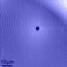
Micropipes are also somehow connected to the growth mechanism of the crystal.
This is neatly illustrated in the picture on the right (taken with a scanning force microscope, courtesy of H. Strunk; Uni
Erlangen) where typical growth spirals are visibly centered around a micropipe. |
|
 |
Micropipes also will definitely kill any device that contains one of them. They
thus must be avoided as much as possible! | |
| |
 |
Let's look at the state of the art of what is around. To quote from the product
sheet of the major SiC supplier Cree, Inc. (located somewhat ironically in Silicon Drive 4600 in Durham, North-Carolina,
USA): |
|
 |
At present, wafer diameters are 50.8 mm or 76.2 mm; doping (usually
with N for n-type and Al for p-type) at high levels produces resistivities in the 0.0x mWcm region. Or there is no doping for semi-insulating stuff. |
|
 |
4H- and 6H-SiC polytypes are sold; for a more
detailed look of some of the products that are available use the link. |
 |
The 2003 state of the art (mostly in the laboratories and
not necessarilly on the market) is summarized in the following table: |
| |
| Diameter | 100 mm
"Four-inch" |
For Si, 100 mm was the standard back in the late 70ties/early 80ties). |
| Defects | Micropipes | < 1 cm–2 for 3''
< 30 cm–2 for 100 mm |
Increasing wafer size usually dramatically increases micropipe density | | Dislocations |
3 · 103 cm–2 achieved | Factor 10 reduction |
|
 |
Of course, in the many laboratories (university and industrial) devoted to SiC,
some data might be even better. |
|
|
|
Electronic Properties |
| | |
 |
The basic electronic properties were listed above
and in an illustration module, here we briefly consider doping and optical
properties. |
 |
First let's ask ourselves a question that should have come up by now: Why is SiC
interesting for optoelectronic applications? How could Siemens
make light-emitting diodes back in 1977 from an indirect semiconductor? |
|
 |
Well, maybe there are bound excitons as
in the case of GaP? Right - maybe! To quote one of the recommended Books
(published 1995):
"The emission (of a-SiC; i.e. probably 6H-SiC)
occurs in a wide band from about 400 nm - 600 nm with a maximum at 480 nm (blue). So far it is not clear what
kind of transition causes the SiC emission". |
|
 |
Now you should be glad: There is something left to do - for you! |
 |
The situation becomes a bit clearer, maybe, by pondering another quote (from a
very good source in Sveden): |
|
 |
" The viewpoint of a crystal grower differs largely from that of a spectroscopist.
The work of a crystal grower is often to provide material of very high quality and sometimes also of high purity. A PL spectrum which may look
excellent for a crystal grower (i.e. shows nothing for an indirect semiconductor), may perhaps not create any higher
emotional feelings for a spectroscopist. Indeed, samples which for a crystal grower may be the outcome of failed experiments
will be the samples of greatest interest for the spectroscopist". |
|
 |
In other words: SiC crystals usually are full of defects with some energy level in
the band gap. Besides the levels form the (usually heavy) doping, and all kinds of exciton levels, there are all kinds of
atomic defects, spanning the range from simple vacancies to impurity atoms and clusters of atomic defects with levels in
the big and roomy band gap of SiC. |
|
 |
There are thus many possible transitions or recombination channels for electron and holes, and some of those transitions might will emit light. |
|
 |
Some more information about the photo luminescence properties of SiC can be found in
an advanced module, here we simply note that the light emission properties
of SiC are not so much a property of the ideal (doped) perfect material, but of crystal lattice defects in a general
sense. |
 |
However: Whatever recombination events produce light - the quantum efficiency
is never very good - the over-all efficiency of the early LEDs was < 1%. Nevertheless, before the advent
of GaN in the nineties, SiC LEDs were the only ones emitting in the blue. |
© H. Föll (Semiconductors - Script)


