 |
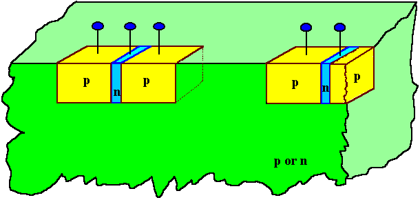
Obviously, embedding the three
slices of Si that form a bipolar transistor into a Si crystal will not do you any good - we just look at it here
to see just how ludicrous this idea would be: |
| |
|
|
 |
What is the problem with this approach? Many points
- The transistors would not be insulated. The Si substrate with a certain kind of doping (either n- or p-type)
would simple short-circuit all transistor parts with the same kind of doping.
- There is not enough place to "put a wire down", i.e. attach the leads.
After all, the base width should be very small, far less than 1 µm if possible. How do you attach a wire to
that?
- How would you put the sequence of npn or pnp in a piece of Si crystal? After all, you have to get
the right amount of , e.g. B- and P-atoms at the right places.
|
 |
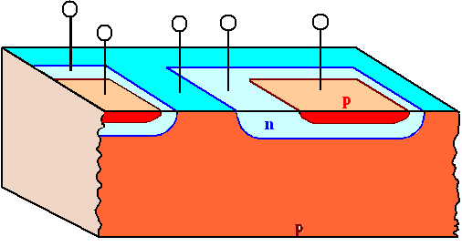
So we have to work with the really small dimensions in z-direction, into the
Si. How about the following approach? |
| |
|
|
 |
This is much better, but still not too convincing. The pro arguments
are:
- Enough space for leads, because the lateral dimensions can be as large as you want
them to be.
- It is relatively easy to produce the doping: Start with p-type Si, diffuse some P into the Si
where you want the Base to be. As soon as you overcompensate the B, you will get n-type behavior. For making
the emitter, diffuse lots of B into the crystal and you will convert it back to p-type.
- The base width can be very small (we see about this later).
|
|
 |
But there is a major shortcoming:
- Still no insulation between the collectors - in fact the Si crystal is the
collector of all transistors and that is not going to be very useful.
|
 |
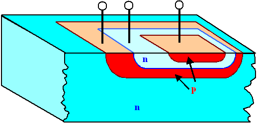
Easy you say, lets add another layer of doped Si: |
| |
|
|
 |
This would be fine in terms of insulation, because now there is always a pn-junction
between two terminals of different transistors which is always blocked in one direction for all possible polarities. |
|
 |
However, you now have to change an n-doped substrate to p-doping
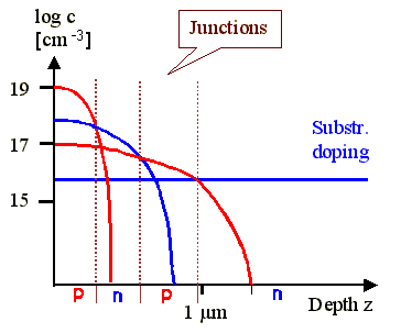
by over-compensating with, e.g. B, then back to n-type again, and once more back to p-type. Lets see,
how that would look in a diffusion profile diagram: |
| |
|
 |
The lg of the concentration of some doping element as shown in the illustration
above is roughly what you must have - except that the depth scale in modern ICs would be somewhat smaller. |
|
 |
It is obvious that it will be rather difficult to produce junctions with precisely determined
depths. Control of the base width will not be easy. |
|
 |
In addition, it will not be easy to achieve the required doping by over-compensating the doping
already present three times. As you can see from the diagram, your only way in the resistivity is down.
If the substrate, e.g., has a doping of 10 Wcm, the collector can only have a lower resistivity
because the doping concentration must be larger than that of the substrate, so lets have 5 Wcm.
That brings the base to perhaps 1 Wcm and the emitter to 0,1 W
cm. These are reasonable values, but your freedom in designing transistors is severely limited |
|  |
And don't forget: It is the relation between the doping level of the emitter and the base
that determines the amplification factor g |
 |
There must be smarter way to produce integrated bipolar
transistors. There is, of course, but this little exercise served to make clear that integration is far from obvious and
far from being easy. It needs new ideas, new processes,
and new materials - and that has not changed from the first generation of integrated
circuits with a few 100 transistors to the present state of the art with some 100 million transistors on one
chip. |
|
 |
And don't be deceived by the low costs of integrated circuits: Behind
each new generation stands a huge effort of the "best and the brightest" - large scale integration is still the
most ambitious technical undertaking of mankind today. |
| |
|
 |
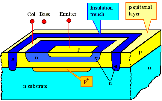
We start with an n-doped wafer (of course you can start with a p-doped
wafer, too; than everything is reversed) and diffuse the p+ layer into it. We will see what this is good
for right away. |
|
 |
On top of this wafer we put an epitaxial layer of p-doped
Silicon
, an epi-layer as it is called for short. Epitaxial means that the crystal is just
continued without change in orientation. The epitaxial layer will always be the collector of the transistor. |
|
 |
Next, we diffuse a closed ring of n-material around the area which defines the transistor
deeply into the Si. It will insulate the transistors towards its neighbours because no matter what voltage polarity
is used between the collectors of neighbouring transistors, one of the two pn-junctions is always in reverse; only
a very small leakage current will flow. |
|
 |
Then we diffuse the n-base- and p-emitter region in the epi-layer. |
 |
Looks complicated because it is complicated. But there are many advantages to this approach: |
|
 |
We only have two "critical" diffusions
, where the precise doping concentration matters. |
|
 |
The transistor is in the epitaxial layer which, especially in the stone age of integration technology (about
from 1970 - 1980) had a much better quality in terms of crystal defects, level and homogeneity of doping, minority
carrier lifetime t, ...) than the Si substrate. |
|  |
We get one level of wiring for almost free, the p+
layer below the transistor which can extend to somewhere else, contacting the collector of another transistor! |
 |
This leads us to the next big problem in integration: The "wiring", or how do we
connect transistors in the right way? |
| |
|
© H. Föll (Electronic Materials - Script)
