 |
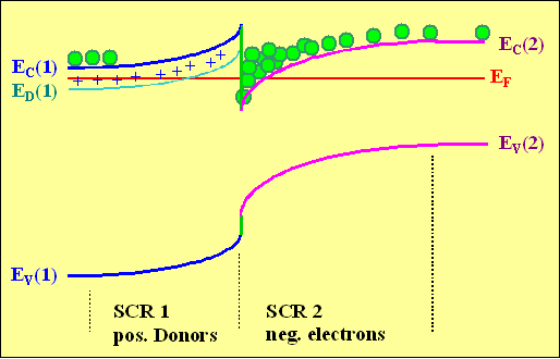
Let's look at the band diagrams of an isotype heterojunction
in equilibrium; we chose a somewhat extreme case: |
|
|
|
|
 |
Electrons were transferred form the (heavily n-doped) wide-gap material 1 to
the (lightly n-doped; almost intrinsic) small gap material 2. Space charge regions form; on the left hand
side by positively charged ionized dopant atoms; on the right hand side by the increased electron density. |
|
 |
In other words: In the low gap semiconductor we have carrier
accumulation
like in Si MOS devices. |
 |
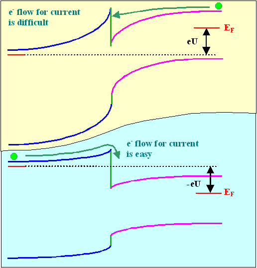
What happens if we apply a bias U? |
|
 |
Well, draw the band diagrams. Move one side up by e · U, and make sure that the band discontinuities do not change. What you get for the structure
from above is shown below. |
| |
|
 |
The current is always carried by majority carriers (electrons in our case). Inspecting the
(exaggerated) drawings, it is clear that this is relatively easy from left to right, but not
from right to left. Without going into the details of the characteristics, there are several novel features emerging
with possible uses for devices. The first one of these effects is clear; the following ones need consideration: |
|
 |
1. We may use an isotype heterojunction to inject majority carriers from the
wide band gap material into the small band gap material as in the case
of diode-type junction. |
|
 |
2. We may use an isotype heterojunction to spatially separate
the carriers generated by doping in the wide band gap material from the doped region. |
|  |
3. We might have peculiar new quantum effects. |
 |
While the first point is relatively clear, including its usability for light emitting devices
(again, try to figure this out yourself), the second and third point
need some explaining. |
| |
|
Modulation Doping |
| | |
 |
Let's look at the isotype junction in equilibrium again
to understand the second point. |
|
 |
What happened is essentially that the electrons missing in the space charge region on the left hand side
were transferred to the potential dip on the right hand side. Of course, electrons are also running down the slope from
the right, but the essential contribution is from the wide band gap material on the left (which, after all, is the cause
for the dip). |
|
 |
Since we picked a highly doped material 1 and a lightly doped material 2, we now have a
lot of electrons (their density is essentially given by the doping in material 1) in a crystal with few
ionized dopant atoms. |
|
 |
And what this means is that we now have a high density of highly mobile electrons,
because the mobility at high doping density is always severely decreased by scattering at the ionized dopants – cf.
the paragraph to this topic. This effect is most pronounced
at low temperatures and can lead to a mobility enhancement of an order of magnitude or even more. |
|  |
This is not only generally useful, but can be carried to extremes. All we have to do is
to make sandwiches as shown below. |
|
|
|
|
 |
With properly chosen dimensions, deep potential wells will form in the low band gap material that contain
most of the electrons from the highly doped wide band gap material. This amounts to a novel way of effectively doping material
2, called modulation doping. |
 |
If the potential wells are small enough (which is usually the case), the confinement
of the electrons in the wells leads to pronounced quantum effects – we therefore call these potential wells "quantum wells" (QW) and distinguish single quantum wells (SQW) and multiple quantum wells (MQW). |
|
 |
An SQW is obtained by sandwiching just one small gap semiconductor, a MQW as shown above.
The introductory picture of the heterojunction subchapter showed examples
of both types. |
|
 |
We may even improve on that by inserting a very thin layer (1 . . . 10 nm, say) of intrinsic material
of a suitable band gap between the two basic materials. If properly done, this layer, while not impeding carrier flow into
the potential wells for equilibration, keeps the carriers from being scattered at the interface and thus increases the mobility
even more. |
 |
But with that we have not yet exhausted the possibilities of heterojunctions – we will
now turn to special quantum effects. |
| |
|
Quantum Confinement Effects |
| | |
 |
Let's consider the peculiar quantum effects in modulation doped structures by looking at some
typical dimensions. |
|
 |
The width of the various space charge layers must still be given by formulas not too different from the
ones we had for Si. For a GaAlAs/GaAs system with a high doping around 1018 cm–3
in the wide band gap GaAlAs side, the width of the dips with the high electron density on the GaAs side is
about 5 ... 10 nm, while the lateral extension is large by comparison. |
|
 |
The mean free path length of
the (highly mobile) electrons is larger than the thickness of the potential dip (better called potential well for the multi-junction
configuration shown above) and this means that we now have essentially a two-dimensional electron gas.
|
 |
What does that mean? Especially if we make the thickness of the layers extremely thin? |
|
 |
It means that we have a periodic crystal in two dimensions (x and y) and a
one-dimensional potential well in the z-direction, which is always the direction used in the pictures above. |
|
 |
The relevant Schrödinger equation is easy to write down, especially in the free electron approximation
with a constant potential (= 0) in x- and y-, and a potential V(z)
in z-direction: |
| |
| – |
 2 2
2 |
æ
ç
è |
1
mx* |
· | ¶ 2
¶x2 |
+ | 1
my* | · |
¶2
¶y2 | + |
1
mz* |
· | ¶2
¶z2 |
ö
÷
ø |
y(r) |
– e · V(z) · y(r) =
E · y (r) |
|
|
|
 |
This equation is solved by |
| |
| y(r) | = |
yvert(z) · ylateral(x,y)
|
|
|
|
 |
The two functions y
lateral(x,y) and yvert(z) are decoupled, the solutions
can be obtained separately. For the lateral part we simple have
|
|
|
| y lateral(x,y) |
= |
Solutions of the two-dimensional
free electron gas problem |
|
|
|
 |
The vertical part of the solution comes frome solving the remaining one-dimensional Schrödinger equation |
| |
æ
ç
è |
– |
 2 2
2mz* |
· | ¶2
¶ z2 |
– e · V(z) |
ö
÷
ø |
yvert (z) |
= Evert · yvert(z) |
|
|
 |
It is rather clear that the structure of the two-dimensional problem will not be much different
from that of the common three dimenional problem if we introduce a periodic potential in (x,y). We simply obtain
Bloch waves in two dimensions instead of plane waves for y
lateral(x,y). The energy eigenvalues are unchanged, too, they were
for the free electron gas (using the effective masses by
now). |
| |
| Elateral | = |
 2k2lat 2k2lat
2m*lat |
|
|
|
 |
The solution of the one-dimensional problem in z-direction depends of course on the precise
shape of V(z), but as a general feature of potential wells we must expect a sequence
of discrete energy levels. For the most simple case of a rectangular well (with infinite height), standard calculations show that
|
| |
| Evert | = |
( p)2 p)2
2mz* | · |
j 2
dz2 |
|
|
|
 |
With j = 1, 2, 3, ... = quantum number, and dz = thickness of the
potential well. |
 |
The total energy of an electron is now given by |
|
|
| Etotal | = |
( klat)2 klat)2
2m*lat |
+ |
( p)2 p)2
2m*z | · |
j 2
dz2 |
|
|
|
 |
This "simply" means that the states in the conduction bands are now a discrete
series given by the quantum number j with a density of states per level of |
| |
| Dlat | = |
 · m*lat · m*lat
2p
| = constant |
|
|
|
 |
If you like to try your hand at a little math: The formula for Dlat is rather
easy to obtain if you follow the recipe for the three-dimensional DOS for this case. |
 |
What do we get from this? Well, a lot of special effects for enthusiastic solid state physicists,
but also some (not necessarily big) advantages for devices. However..... |
|
 |
Each quantum well
layer is now something like a one-dimensional atom
– in contrast to the three-dimensional real atoms were the wave functions of the electrons were confined in all three
directions. If we move these "atoms" close together in the z-direction, there must be a point where
the wavefunctions in z-direction (the yvert(z)) start
to overlap and do all the things real atoms do at close distance. |
|
 |
The energy levels change and split, and – in analogy to a crystal formed by real atoms – a
one-dimensional energy band may start to develop with an energy range that is given by the geometry
of the system, i.e., the thickness of the layers, for a multi quantum well structure. |
| |
This is a momentous statement! Think about it!
|
|
 |
It means that we can make materials with energetic properties that we can tailor at
will (within bonds and limits, of course). We no longer must just live with bandgaps and other properties that
mother nature provides, we now can make our own systems. At least in principle. |
|
 |
Something like that we call a metamaterial. |
|  |
Multiple and single quantum wells are already part of recent devices as shown in the last
module of this chapter. |
|
| |
© H. Föll (Semiconductors - Script)

