 |
The expressions "Thin films" and "Semiconductor technology"
are almost synonyms. It is true, there is some semiconductor technology that does not need thin films but not much comes
to mind right away. |
|
 |
There is, however, quite a bit of thin film technology outside of semiconductor
technology, e.g., in optics. In fact, thin film technology is far older than semiconductor
technology. In ancient times, for example, people already knew how to beat gold into a thin film (< 1 µm
thickness) with hammers and knew how use this "gold leaf" for coating all kinds
of stuff. |
|
 |
When you wax your car, or paint a wall, you are actually applying a thin film - or
are you? |
 |
How thin does a thin film have to be to fall
under the notion of "Thin Film"? The "Ohring", for example doesn't tell you. The "Smith" doesn't give you a number either but offers the following working definition: |
|
 |
Thin film technology involves deposition
of individual molecules or atoms.
Thick film technology involves deposition of particles. |
|
 |
Painting thus is thick film technology, and evaporation
is thin film technology. Good enough, but what about beating gold with hammers to sheets with a thickness of 5 nm?
Or depositing 100 µm of Ag or Cr on a metal galvanically? - atom by atom, to be sure. |
 |
All in all, there is no natural distinction between "thick" and "thin",
it always has to be practical. In what we look at here, we consider in a first approximation thin films to by typically
thinner then 1 µm, or if needs be a few µm. Let's get an idea of what that means: |
|
 |
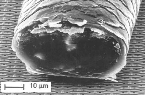
One of the smallest things we still can see
and touch is a human hair. They come fine and coarse, but a typical thickness
value is (30 - 50) µm as you can see below. |
|

Human hair on top of a 4Mbit DRAM (around 1990) |

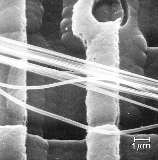
Spider "silk"
on top of memory chip.
One strand consists of several rather fine strings. |

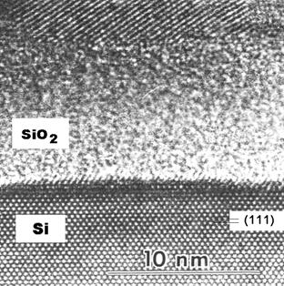
Thin layer of oxide on Si (with poly-Sion top);
atomic resolution. About 10 nm thick |
|
|
 |
We we can also see the strands of a spider web. Yes - but only because what we see is a bundle
of many strings with diameters > 1µm. An individual string would be rather invisible to us humans. |
|
 |
If we look at a Si wafer covered by 10 nm of oxide we see - nothing whatsoever.
It looks exactly like a Si wafer with no oxide; at best there might be just a hint of some greyish-brown hue. |
 |
So the word "see" is of interest
here. If you can see it - it may not be "thin".
The number to remember is the wavelength of light: <» 1 µm |
|
 |
That simply means that if its's smaller than roughly 1 µm in all dimensions, you
can't see it anymore. |
|
 |
This is not quite true, of course, if something is only < 1 µm in one dimension,
i.e. if we have a thin film. We all have seen interference colors from
thin oil films on water; the thickness then is only some fraction of the wavelength
or well below 1 µm. Actually, the color you see from an otherwise completely colorless and transparent thin
film is directly coupled to its thickness - we have a first method to actually measure
the thickness of a thin film |
|
 |
Class Exercise:
How was that? Interference causes the color of a thin film and betrays its thickness?
Use the link for a reminder. |
 |
OK - so if we want to "see" more than interference effects, we must
use electron microscopes. That's a simple but costly first conclusion.
Let's buy a scanning
electron microscope or SEM (take out € 200.000 - €
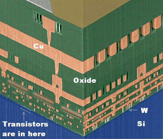
400.000 from your savings account) and look at the cross-section of a modern IC, a cut-open chip: |
| |
 | Cross-section of modern chip; colors are artificial.
Picture courtesy IBM |
|
|
 |
The first thing to note in the picture above is that IBM did not provide a scale. For
a Materials Scientist this is not acceptable (=failing grade if you provide a picture
without a scale). However, the size of the letter "W" (=tungsten) is about 1 µm so you get
the idea that there are a lot of (still) thin layers involved. There are actually far more thin films than meet the eye
in this picture; just wait. |
 |
Anyway, you now have a first impression of the realation between thin films and
semiconductor technology. Now let's look a bit more detailed on the meaning of "thin". |
| |
|
The Meaning of "Thin" |
| | |
 |
Again, we say layers are thin if their thickness dz <
d0 with d0=5 µm for example. |
|
 |
This is a fine definition (and implicitly used a lot), but it is also arbitrary. Why 5
µm and not 0.1 µm or 10 µm? Well, quite often, without thinking too much about it, dz
is scaled with other typical geometrical dimensions. If we look at a single transistor in a modern integrated circuit, its
lateral dimensions are in the 1 µm region, and we certainly would demand that d0 must
now be smaller than this if we consider thin films on top
of the transistor. |
 |
From this example, we get a clue for a good alternative but qualitative definition
that helps to keep our perception of thin films focussed: |
|
 |
A film is thin if its thickness is in the same order of
magnitude or smaller than some intrinsic length scale of the system we are considering. There
is a surprisingly large number of such length scales; let's look at a few in the context of semiconductor technology: |
| |
| Intrinsic length scale |
Magnitudes | Remarks | | Structural Scales
| | Geometric dimensions dx, y, z |
Any; "Thin" if dz « dx,y |
Trivial. | | Changes in dimensions |
Dd »
e · d | Thermal expansion; other stress / strain sources
e=strain |
| Grain size dgrain | nm - cm |
Strong influence on mechanical and electrical properties |
Other internal structural sizes
(e.g. phases in multi-phase compounds). |
From nm to > 10 µm | Important in proper context |
| Roughness amplitude. | | Interfacial layer thickness. |
| Radii of curvature. |
| (Average) distance between dislocations or other defects. |
| Lattice constants a0 | (0.3 - ...10) nm |
Ultimate limit. dz < a0 doesn't make sense |
| Wavelength Scales |
Wavelength of interacting radiation
- Light (including IR and UV)
|
» 5 µm - 0.2 µm |
Determines what you "see" |
- X-rays
- Electron beams
| "»" nm |
Internal wavelengths l
- Electrons in conduction band.
- Quasiparticles
(phonons, excitons, plasmons, polarons, polaritons, Cooper pairs, ... |
You don't have to understand that here. |
What happens if dz > » l |
| Interaction Scales |
Absorption depths
- Light
- Electron beams |
- km (glass fibers) - nm (metals)
- nm - few µm |
|
Mean free paths'
- Electron scattering |
» 10 nm - 1 µm | |
Diffusion length of minorities
| » 10 nm - 1.000 µm | |
| Electrical Scales |
| Space charge region width dSCR |
» 10 nm - 10 µm | |
| Debye length dDebye | 0.1 nm (metal) - m
(insulator) | | | Scale of doping gradients |
» 10 nm - 10 µm | |
| Critical thickness for electrical break down |
» 1 nm - 100 µm | |
| Critical thickness for tunneling |
< » 5 nm | |
|
 |
Wow! Lots of scales - some you (should) know, some will be new. There are even
more internal scales, but what we have is enough to get a feeling for: |
|
 |
1. "Thin" is indeed a relative measure. |
|
 |
2.
Properties of thin films might be quite different from that of the bulk material
if that property is some expression of an internal length scale.. |
|
| |
|
The Meaning of "Film" |
| | |
 |
After we have defined (or confused) the meaning of "thin",
we will now ponder the meaning of "film". |
|
 |
What we don't mean is the (thin) film of
water on your wet windshield, nor do we mean the layer of dust on your furniture. While
thin films of liquid might be legitimate objects of thin film semiconductor technology, and the avoidance of thin films
of dust is in fact a major topic in semiconductor technology, in this lecture we concentrate on
- Solid films: single crystalline, poly crystalline, amorphous; whatever.
- Adhesive films: There is some bonding at the interface,
i.e. the thin film does not easily disattach from its substrate.
|
 |
That's all. We might go a bit further and demand that the thin film has about
the same thickness everywhere, and that it should be homogenous (same properties everywhere), that it should not contain
holes or cracks, and so on. But this is either a matter of course or a legitimate special topic in thin film technology
that needs to be treated on its own merits. |
© H. Föll (Semiconductor Technology - Script)
