| Single Crystal Silicon
|
 |
Here are a few pictures of the biggest and most perfect crystal that is known
on this side of Jupiter. |
| |
|
|
|
 |
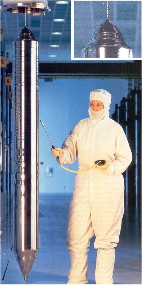
| Freshly grown Si single crystal with 200 mm diameter |
| The inset shows the top part of the crystal, showing that the » 150 kg
heavy crystal is hanging on a seed crystal just a few mm in diameter. |
| Some Smithsonian magazine (?) |
|
| | |
|
 |
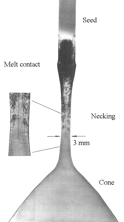
The thin neck is absolutely essential for growing a dislocation-free crystal.
Below is a rather amazing picture where we look with X-rays into the neck region of a silicon crystal in such a way that
we see dislocations as thin dark lines. |
| |
 |
When you dip your already quite thin seed crystal into the hot melt (1410 oC; 2570oF)
, the thermal shock generates stress, and stress generates dislocations at this temperature quite easily. You can't avoid
that. What you do then is: First pull rather fast. The diameter of the growing crystal will then decrease to a few mm. This
is the "Dash process", invented by W.C. Dash in 1958,
"just in time". The trick, in a nutshell, is to pull faster than the dislocations can move. That demands a very
thin crystal, and as the picture shows, it works! The dislocations move out to the surface and eventually the growing crystal
is dislocation free. Then you slow down and increase the diameter to whatever you need, e.g. 200 mm or 300 mm.
This
"necking procedure", or the "Dash necking process" is one of the many little marvels that enabled silicon
technology. Of course, the first law of
economics still applies. You end up with a huge and heavy (up 250 kg) crystal hanging on a thread or better threat!
If the thin neck breaks while you are pulling, and your already grown crystal plunges into the hot melt, you better start
running fast. You must outrun either the exploding machine or your boss, who will try to get you for destroying equipment
worth millions! |
| | |
|
|
|
 |
X-ray "topograph" picture showing what happens during
Dash's "necking" procedure |
| Source: Courtesy of Wacker / Siltronic; Burghausen, Germany |
|
| | |
|
 |
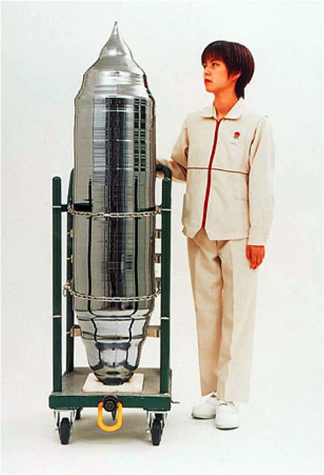
Here is one of the humongous 300 mm diameter Si crystals mass-produced today (2011): |
| |
|
|
|
 |
| Silicon single crystal with 300 mm diameter |
| Source: Courtesy MEMC. |
|
| | |
 |
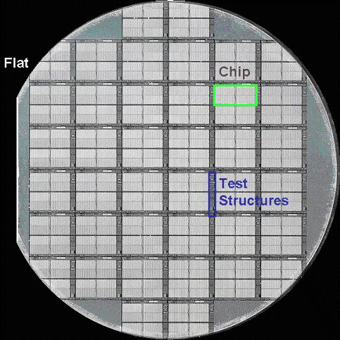
The cylindrical part of these crystals will be cut into discs that are subsequently
ground and polished to the ubiquitous silicon
wafers as shown below. |
|
 |
Now you have the starting material for all kinds of "micro"-electronic
nano devices, like all your electronic stuff, power managing components, solar cells, and not to forget, MEMS
products like the acceleration sensors and gyros in your car and your i-phone, or the light-processing chips with millions
of tiny mirrors in your beamer. |
| |
|
| |
|
| | |
 |
These silicon single crystals do not contain a single dislocation.
They are - so far - the only big crystals that we can make completely free of dislocations. Germanium (Ge) crystals can
be pretty good, too, but are not quite as perfect as silicon crystals. They are also far more expensive since "raw"
germanium is expensive. |
|
 |
That is an extraordinary occurrence! Microelectronics needs materials with some special electronic
properties and rather perfect, large, dislocation-free crystals of that material. Germanium
doesn't meet the electronic specifications (not to mention cost considerations). Gallium arsenide crystals or other "III-V's"
good enough for making electronic components like LED's or Lasers are rather expensive but far less perfect than silicon
and never dislocation free.
It is a kind of amazing coincidence that the basic properties of silicon meets all electronic
specifications admirably and that it is the only
material that can be grown into huge and nearly perfect single crystals!
Those
crystals are also extremely clean. Besides a few doping atoms (As, P, or B) incorporated intentionally at precisely determined
concentrations, they only contain some dissolved oxygen (a few ppm), and somewhat less than 1 ppm carbon. Those impurities
are tolerated or even helpful. Everything else is far below the ppt level |
 |
By the way, there cannot be such thing as a fully
perfect Si crystal. Even the most perfect ones must by necessity contain a low density
of small clusters of vacancies and self-interstitials.
Why? Consult this
link to find out. |
| | |
|
© H. Föll (Iron, Steel and Swords script)
