|
The Story of Self-Interstitials in Silicon |
 |
After electron tubes went out of style around 1970, the word "electronics"
became more or less synonymous with "silicon devices". Silicon devices like microprocessors, memories, solar cells,
or power handling devices like thyristors, are made by diffusing certain substitutional
impurity atoms into precisely determined regions of a silicon crystal. Silicon
technology and thus "electronics" is based on diffusion,
and diffusion of atoms in crystals, as the reigning dogma stated, needed vacancies.
In the beginning of silicon technology nobody had a problem with that because nobody expected any problems. Why shouldn't
things in silicon not be like in all other simple cubic crystals, where atoms were certain to diffuse via vacancies? |
 |
However, before one can start to make a silicon device by diffusing impurity atoms
like phosphorous, (P), arsenic (As) or boron (B) into the silicon, one needs to make a silicon
crystal first. Not just any silicon crystal but a rather large and rather perfect single
crystal, absolutely free of dislocations and, as far as possible, of precipitates or other small clusters of something.
|
|
 |
Fortunately, making rather perfect crystals is possible with silicon. Actually, it is only possible with silicon (and to a lesser extent with germanium (Ge)). Rather large dislocation-free
single crystals of silicon can be "pulled from the
melt", using all kinds of ingenious tricks, and these crystals produced a completely new situation concerning vacancies
in equilibrium. As in all materials, vacancies must be present in the equilibrium concentration right after solidification. As the freshly solidified material cools down,
the equilibrium concentration of vacancies decreases exponentially, and the vacancies no longer needed must "disappear".
This is true for all crystals. Getting rid of surplus vacancies is no big problem in almost
all crystals since the vacancies only need to move to the nearest dislocation, grain boundary, or whatever "large"
defect is nearby, where it can get absorbed and thus effectively
withdrawn form the free vacancy population.
The exception are the perfect silicon crystals that do not contain large
defects that could absorb surplus vacancies. So with the advent of big perfect silicon crystals, a new question came up:
How can the silicon crystal get rid of its surplus vacancies while it cools down? |
|
 |
Good question - but still no problem. The surplus vacancies simply would cluster and form
larger aggregates. Either three-dimensional voids or, if they
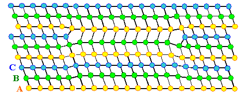
form a platelet, little dislocation loops with stacking faults inside as shown
here. That kind of stuff had been seen in other cubic crystals and there was still no need to worry. |
 |
So when silicon crystal growers did indeed find some small defects in their crystals,
made visible by some tricky etching procedure, nobody worried
much. Here are some pictures of what I'm talking about: |
| | |
|
|
|
 |
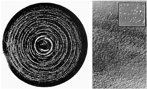
| Swirl defects in silicon made visible by defect etching |
| The picture on the left shows a cross-section of a 5 cm crystal. The picture on the right shows
a closer (optical microscopy) view of the pattern; the "dots" in the inset are about 1 µm in size. |
|
| |
| |
|
 |
On the left hand side a complete defect-etched wafer is shown (with only about 5 cm diameter
in these early silicon times); on the left we give one of those "spiral arms" a closer look. Essentially there
are a lot of tiny (around 1 µm) features on the surface, that resulted from etching-out some defect that was supposedly
some vacancy cluster.
The fact that all these defects were arranged in a kind of spiral pattern didn't worry anybody;
this could be understood in principle by looking at the nucleation of
these defects in conjunction with the special crystal growth conditions. The spiral pattern thus only inspired the name
"swirl defects" for this special kind of "vacancy clusters". |
 |
All that was needed (for perfectionists) was to look at some of those defects
in an electron microscope, just to make sure that they were
indeed the vacancy clusters that we all knew they must be. Unfortunately, the density of those things was far too small
for a random search. You were not likely to find one of those guys in a random specimen taken from the silicon crystal,
since the volume one can investigate in an electron microscope is so small. It's like searching for a lost contact lens
in a base ball field by looking with magnifying glasses at one square foot a day. You are not going to find it very quickly.
Of course, after defect etching you knew where you should have looked - but now the defect was gone. |
|
 |
Well, some guys at Siemens around Dr. Bernd O.
Kolbesen, my good friend ever since, succeeded in preparing some specimen where one could find those defects
in an electron microscope (albeit not without a lot of work and frustration) 1).
For those samples one needed a special high-voltage electron microscope, of which there were only two in all of Europe -
and I was the guy who had access to one of those monsters in 1974. We got together, did the work, and found that swirl defects
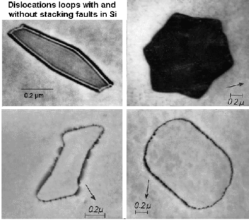
looked like this: |
| |
| |
| |
 |
 |
Observed swirl defects and a schematic lattice model of a
vacancy type dislocation loop with a stacking fault. |
|
| |
| |
 |
That was still fine - what we have are dislocation loops around some stacking
fault (upper row) and loops without stacking faults (lower row). They were a bit on the big side, but so what. The fact
that some loops had no stacking fault was also easily understood
within conventional dislocation theory, and there was still nothing to worry about. |
|
 |
What one needs to know now is that in principle, interstitial atoms could do pretty much the
same thing as vacancies. They could cluster in a plane producing a dislocation loop with a stacking fault. A schematic drawing
corresponding to the one above but showing interstitial-type clustering is shown in
this link. If imaged under usual conditions, these interstitial
type dislocation loops would look pretty much like the ones shown above. |
|
 |
The pictures above thus only show that there are the expected kinds of dislocation loops,
but not if they are of the vacancy type or interstitial type.
Fortunately, there
is a way of telling. It involves a bit of tricky electron microscopy (rather error prone), and after we improved the way
to do this2), we analyzed a number of those loops and found to the utter amazement
of all involved: |
| |
| |
| |
Swirl defects are
interstitial type dislocation loops!
|
|
| |
| |
 |
Surprise! It sure looked as if self-interstitial are the dominating point defects
in silicon, and not vacancies, as automatically assumed (for good reasons, to be sure!)
by all and sundry - except for my Boss: Prof. Alfred Seeger. Together
with a guy named Chik he had analyzed diffusion data and postulated that in silicon the self-interstitial would be involved
in a major way in the diffusion of atoms. |
|
 |
In the small world of silicon material scientists this was a rather momentous discovery, in
particular because it gave substance to Seeger's claim that diffusion in silicon would proceed via some mechanism mediated
by self-interstitials and not vacancies.
Momentous discoveries like this always receive the same treatment from one's
peers: the whole thing is doubted and ridiculed. Just look at the Nobel-prize winning discovery of quasicrystals
for another example. However, since others eventually corroborated our findings, self-interstitials became eventually accepted
as major point defects in silicon. It only was forgotten to give us the Nobel prize, unfortunately. |
 |
Where do we stand today? Well - the final word is not yet in.
There is no doubt anymore that both vacancies and self interstitials occur in silicon with relevant concentrations, and
that diffusion does involve self-interstitials at least in some cases. However, things turned out to be far more complicated
than "naively" expected in an "only vacancies" or "only self-interstitials" kind of picture,
and we still do not have good basic data like the formation and migration
energies for vacancies and interstitials in silicon. |
|
 |
The problem is that it is exceedingly difficult to measure experimentally exactly what is
going on. The classical methods for looking at point defects directly
completely fail in the case of silicon, and the more indirect methods are mostly ambiguous.
Like with electron microscope
pictures of dislocation loops, measurable things in diffusion often look pretty much the same for both possible mechanism:
diffusion via vacancies or via interstitials.
To be sure, various high-powered groups of scientists have suggested
definite numbers and mechanisms but the final word has not yet been spoken. It will not take much longer, however, because
in the not too distant future we will simply be able to calculate all that stuff. Ironically, this will be possible since
silicon chip complexity and therefore computing power keeps growing despite the fact that we do not fully understand what
we are doing when we make chips by employing diffusion of atoms in silicon. |
| |
|
© H. Föll
© H. Föll (Iron, Steel and Swords script)
