 |
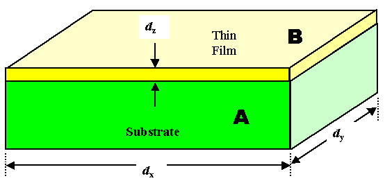
Once more, what we want to have - idealized - is shown below. A thin film of a
material A on top of material B. Of course, as we have seen, the interface (and thus the surface of material
B) does not have to be perfectly flat but can be somewhat rough or even extemely rough. |
| |
|
 |
But now we look at the quite important parameter
of adhesion. What does that mean? |
|
 |
It is obvious. Thin films A that do not adhere
to their substrate B will not be of much use, since they will come off with little force. |
|
 |
We have a first problem. Let's say you want a thin film of Teflon on top of your semiconductor, or whatever. Maybe not you
personally, but lots of other people would just love to have that. Unfortunately, as we all know, nothing sticks
to Teflon. In other words: The sticking coefficient of Teflon molecules (whatever
exactly that will be) to any substrate is close to zero. |
|
 |
There is indeed such a thing as a well-defined sticking coefficient of B
on A, and we will come back to this. |
 |
Adhesion is thus a relatively clear thing, easy to conceive, and what we worry
about now is how to define and measure it in some quantitative way. This is relatively easy, too - in principle. |
|
 |
A direct measure of the amount of adhesion that we have for some interface is
the work or energy we need to employ per cm2 to remove B from A. This is nothing but the
good old concept of surface and interface energies,
applied to thin films, i.e. interfaces between two different materials. The questions now coming up are:
- Can we calculate the interfacial energy between A and B?
- Can we measure the interfacial energy between A and B?
- Is it always the same, or does it depend on, e.g., the thickness dZ or the detailed structure
of the interface between A and B?
|
 |
Let's look at the answers: |
 |
Can we calculate the interfacial energy between A
and B? |
|
 |
Not really. Or better put: That depends on many things. If we know the exact
nature of the bonding between A and B, and if we can do all the calculations required, we will get relatively good results.
|
|
 |
But even without calculations, "theory" can give us a lot of important
inputs. The interfacial properties, as far as adhesion is concerned, come just as much from the bonds and their binding
potentials in the interface between A and B, as most of the mechanical
properties of pure A or pure B. Essentially the same rules apply. |
 |
A few examples for this: |
|
 |
If you deposit a metal B on top of a metal A and you know from
the phase diagram that these metals are completely
miscible, you know that you will have no adhesion problem. Complete miscibility, after all, necessitates
that the bond strength between A-A, B-B, and A-B is not too different, so your A-B bonds in
the interface should be just about as strong as those in A and B. |
|
 |
The same kind of thinking will tell you that Si on Ge, for example,
or any III-V semiconductor on top of any other covalently bonded group IV, or III-V semiconductor should
give good adhesion. |
|
 |
The same kind of thinking, however, will also teach you that if there is just
one molecular layer of "dirt" in between A and B, you might
be up shit's creek, as the saying goes, because you don't know how A and B bond to "dirt".
|
|
 |
Everyday experience also tells you that if there is not a continuous layer of
dirt in between A and B, but just some dirt particles (called e.g. dust), you simply will not get A-B
bonding either. And now you even realize that just a few particles of less then 1 nm in diameter or some roughness
of the two layers before they make contact will already be enough to prevent bonding between A and B on an
atomic scale. After all, if you put a macroscopic piece of metal A on top of a metal B the adhesion will always be zero.
|
|
 |
Things of any kind, brought into what we think is "close contact" do
practically never stick together, and we sure are glad for this! |
|
 |
That leads straight to a trivial, but important insight: Not counting some exotic
techniques ("Wafer bonding"), we never produce a thin film by "putting"
the film B on A. |
|
|
Thin films are always grown
on their substrate |
|
 |
Now to the second question: Can we measure the interfacial
energy between A and B? |
|
 |
Yes, of course - but... . Let's look at the "standard" techniques first.
Essentially you try to delaminate your layer by "pulling" or "pushing". Measuring the force needed to
do that gives you a quantitative number that you may be able to convert into the interfacial energy. |
|
 |
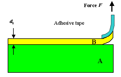
The simplest technique is to attach an adhesive tape ("Tesa") to your
layer. If there is better adhesion at the interface tape- layer than at the interface layer-substrate, you might be able
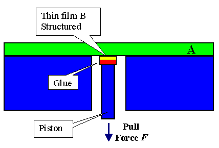
to pull off your layer as shown. Or you make a hole in the substrate and push up with a small piston, or you pull down the
piston after glueing it to the thin film. |
|
|
|
|
 |
If you can structure your layer as shown in the second picture, you could glue
some "piston" to it and try to pull the layer off |
 |
If that looks pretty unconvincing - that's because it is! Imagine doing that to
a 5 nm film. You won't even be able to see if anything is doing. |
|
 |
Nevertheless, these techniques often work, and, of course, we can conceive of
more sophisticated versions, too. But quite often you must admit defeat. You just can't measure the interfacial energy of
your thin film easily or at all - in particular if their is very good adhesion, i.e. a high interfacial energy. |
|
 |
The good news in this case, of course, is that you don't care much then. |
 |
We have one question left: Is the interface energy always
the same, or does it depend on, e.g., the thickness dz or the detailed structure of
the interface between A and B? |
|
 |
What do you expect? Of course it does, at least to some extend. A soon as we
look at epitaxial growth, we will see what might happen in interfaces and how it
relates to its energy. |
© H. Föll (Semiconductor Technology - Script)


