|
Photonic Crystals |
| |
Waves Moving in a Periodic Potential and Photonic Crystals |
 |
Let's start with refreshing your memory about waves by clicking on this icon:
 |
|
 |
Now that you are back, let's recall a few basic properties of plane waves, the
most simple waves there are, just travelling around in an environment that doesn't do anything to them. Think of a light
wave in vacuum, for example. What we have is
- The amplitude A giving the "strength" of the wave.
- The wavelength l, telling on what space scale
the wave repeats itself. A better quantity is the
- Wave vector k, giving the direction of propagation and the
wave length via |k| = 2p/l
- The frequency n or its inverse, the cycle time T = 1/n,
telling on what time scale the wave repeats itself.
- The momentum p = hk/2p with h = Planck's constant.
- The energy E = hn
- The propagation speed v = nl
|
 |
Now let's look at what happens if this wave now encounters a medium that interacts
with it in a periodic way. |
|
 |
Consider electron waves. An electron in vacuum just flying by with some speed
is described as a plane wave exactly as light waves. The only difference is that its amplitude is not given in terms of
an electric and magnetic field as for light waves, but in terms of a "wave function" called y.
A medium that interacts with an electron wave in the most simpel possibel way is an atom; any atom will do. A medium
that interacts with an electron in a periodic fashion is an arrangement of atoms in a periodic fashion. Atoms that are arranged
in a periodic fashion we call "crystal", of course. |
|
 |
So let's take an electron (wave) from any electron gun (as found in old-fashioned
picture tube TVs) and shoot it into a crystal. On second thought, since old picture-tube electron guns are hard to get today,
let's just take an electron that already happens to be inside the crystal and moves around freely, like in a metal or semiconductor.
Since all electrons are equal (really!), you can't tell an electron that was shot in from one that was always inside.
Electrons that happen to have wavelengths that "scale" with the "wavelength" of the periodic disturbance
will experience an effects we call diffracted, exactly like suitable X-rays. Time to
refresh you memory once more by going to the module in the margin. |
|
|
|
 |
"But that was about X-ray diffraction", you might complain. "Here
we discuss electrons, an entirely different animal".
You are right. Nevertheless, electron waves, X-ray or electromagnetic
waves, those unpleasant sound waves emitted by the Ghettoblasters of your offspring that can sterilize frogs up to a distance
of 50 feet, waves in water, and whatever else waves around, do all exactly the same thing since their mathematical description
is the same (except for some unimportant details). Any plane wave writes: |
| |
|
| | |
| A(x, t) |
= | A0 · sin |
æ
ç
è |
2p · |
æ
è | x
l | – |
n · t | ö
ø
| ö
÷
ø |
| | | |
| | |
| | |
| | | |
= | A0 · sin |
(k · r – w
· t) | |
In three
dimensions
with vectors |
| | | |
| | |
| | |
| | |
= | A0 · exp |
{i(k · r – w · t)} |
| in complex
notation |
|
A = amplitude = electrical field strength for electromagnetic waves, pressure for sound waves,
and so on.
k = "wave vector" = 2p/l; w = circle frequency = 2p · n;
r = position vector; i2 = –1 = imaginary unit. |
|
| |
| |
|
 |
Any plane wave gets diffracted at some periodic disturbance; exactly how is covered
in the X-ray diffraction module. |
 |
Here we look at the situation from a different angle. A (transparent!) periodic
disturbance, put in the way of waves with all kinds of wavelengths and directions, acts like a filter.
Most waves pass right through; it's like the object causing the periodic disturbance is not there. However, waves with a
fitting "geometry" (given by their wavelength and propagation direction), get diffracted. That means they change
their direction radically.
The diffracted wave, as long as it propagates inside the periodic medium, gets diffracted
again and again - the total effect is that a standing
wave is formed. |
|
 |
That would not be all that remarkable yet. The important thing is that those diffracted
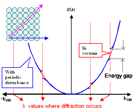
(standing) waves "change" their energies - even so they do not change their wavelengths. That is shown below: |
| |
| |
| |
 |
| Energy splitting at wavelengths (or k values) where diffraction occurs |
|
| |
| |
|
 |
Shown is the energy E(k) of electron waves as a function
of their wave vector (or inverse wavelength, if you like that better). Imagine waves running along the two directions indicated
in a simple cubic crystal. Without crystal, their energy would be proportional to the
square of the wave vector k; this is shown by the red curve.
With crystal, the (blue) energy curve is interrupted for special k-values
and deviates a bit for neighboring values, too. |
 |
What does it mean? That inside a crystal electrons cannot have all
possible energies as in vacuum, there are energy gaps! Some energies are not allowed. Electrons with the "wrong"
energy can simply not exist inside a crystal.
This is, of course, where semiconductor science starts. |
|
 |
If you "shoot" an electron with a "wrong" energy into a crystal,
it cannot move in there. All kinds of strange things must now happen - in contrast to an electron with the right energy
that (more or less) just keeps moving! |
 |
Why do I test your patience with slightly weird concepts of electron waves running
around in a crystal or periodic potential, to give it its correct name? Because the
theory of what happens then had already be developed to an extreme level of complexity (as needed for todays semiconductor
devices) before somebody came up with the idea to carry this over to optics, i.e. to
simple electromagnetic waves with wavelengths just below 1 µm. |
|
 |
As always, two guys had similar ideas at about the same time. Eli Yablonovitch
and Sajeev John published their "photonic crystal" milestone papers in 1987 |
|
 |
Why did it take that long? Well - how would you make a periodic disturbance in
three dimensions that is just right for light? In other words: something with a periodic
change of the index of refraction on a scale of 1 µm or even smaller?
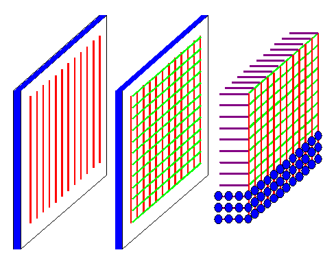
In one dimension it had been done for a long time. In the good old times we called that a diffraction
grating; now we might call it an one-dimensional photonic crystal.
It's easy to illustrate this - I can use an old picture: |
| |
|
| |
 |
| Diffraction gratings or photonic crystals in 1, 2, and 3
dimensions |
|
| |
|
|
 |
Mother nature has made three-dimensional diffraction gratings for
us in the form of crystals. The "wavelength" (or better lattice constants) of those crystals is below 1 nm, and thus just right for those electron waves or X-rays.
Unfortunately, it is far too small to do anything special with light. |
 |
Since most of us are not as smart as Mother Nature, we had (and still
have) big problems making two and three dimensional "photonic crystals" with lattice constants around 1 µm.
As it turned out rather late, Mother Nature had mastered that problem, too, long ago. |
|
 |
Opals
and some wings of butterflies or other bugs are natural photonic crystals in more than one dimension! Then we have pearls
and pearlite, of course.
The link shows why opals are photonic crystals. If you admired colorful iridescent wings or
body parts of bugs, chances are that you looked at natural photonic crystals, too. This already shows that photonic crystals
make for exciting colors. |
| |
| |
| |
Some Remarks About Photonic Crystals |
 |
Why did people (well, some of them) get so excited about photonic crystals in
recent years? Because they would offer a lot of new and exciting possibilities to make money, or at least to gain some recognition
as a scientist. |
|
 |
First, just looking at the parallels to what
electrons do in periodic potential, the concept of all-optical chips, doing whatever electronic chips do, just better and
faster, was born. While true in principle, we still need to wait for those chips to appear.
Second, all kinds of unusual and interesting optical effects emerged. This is still
very much en vogue - but a completely new thing came up too:
Third, with photonic crystals one could produce so-called meta-materials (something
Mother Nature failed to provide us with) with completely new and rather crazy properties. They could have a negative
index of refraction, for example! If you know anything at all about the index of refraction, your mind must now have boggled.
With these meta-materials one could not only make perfect lenses but (in principle) also those devices loved in science
fiction books (and in old sagas): invisibility cloaks or helmets!
|
 |
I spare you fourth, fifth, and so on, and only give you one idea about how one
could make photonic crystal. Nowadays we have many ways for doing that, all of them rather ingenious. |
|
 |
What I will show you here has the disadvantage that it is not among the major
and promising methods. The advantage is that it was to some extent developed in my group and by groups we collaborated with.
The method employs the etching of tiny pores into semiconductors, in particular silicon, in conjunction with standard methods
for micro / nanostructuring as known from microelectronics.
The link provides for far more detail about pore etching
in semiconductors then you ever wanted to now .
Let's just look at some results here: |
|
|
| |
| |
| |
 | | Two-dimensional photonic crystal "in" silicon |
| Source: MÜLLER, F., BIRNER, A., GÖSELE, U., LEHMANN, V., OTTOW, S., FÖLL, H.: Structuring
of macroporous silicon for applications as photonic crystals. J. of Porous Mat. 7 (2000) 201-204 |
|
| |
|
|
 |
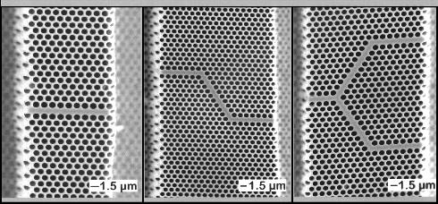
Here are some details from similar structures: |
| |
|
| |
 |
| Two-dimensional photonic crystal "in" silicon with "defects" |
|
| |
| |
|
 |
The rows of missing pores are defects in the photonic crystal. Ligth can pass
along those defects and you have now a possibiltiy to "process" light in very small dimensions. |
 |
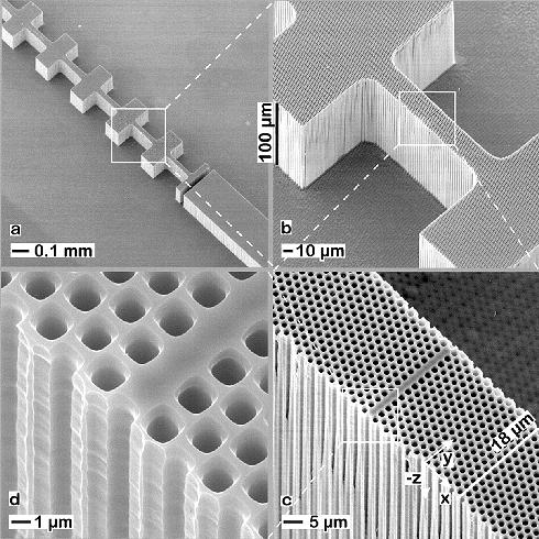
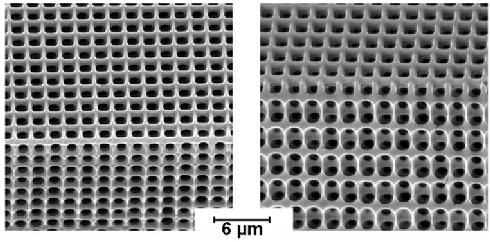
In the group of my late and lamented friend Ulrich
Gösele, the technique was carried to extremes as shown here: |
| |
| |
| |
 |
| Three dimensional photonic crystal "in" silicon
made by pore etching |
Source: From U. Gösele's group.
Similar pictures can be found in: Andreas Langner, Frank Müller, and Ulrich Gösele: "Macroporous
Silicon" in a Springer Text Book about “Molecular- and Nano-Tubes”. |
|
| |
| |
|
 |
I guess you can understand that besides all the official reasons for researching
photonic crystals, there is also an unofficial one: it's fun! |
 |
Why did I write this module? Because pearlite is called pearlite
because it has a pearl-like luster; and pearls have their luster because the nacre they consist of is actually a two-dimensional
photonic crystal. |
|
 |
I also like to show off on occasion, of course. |
| | |
|
© H. Föll (Iron, Steel and Swords script)
