| |
5.3.2 Phase Boundaries |
 |
Now let's look at phase boundaries, the
second important two-dimensional defect. |
|
 |
Like a grain boundary it has two sides but now different things (or, as we call
it, different phases) are separated by a phase boundary. After all, our iron comes in
more than one phase and on occasion we have both phases simultaneously.
Between two atomically connected phases we then must have a phase boundary by definition.
|
 |
You have seen a lot of phase boundaries. Or maybe you didn't. There are none so
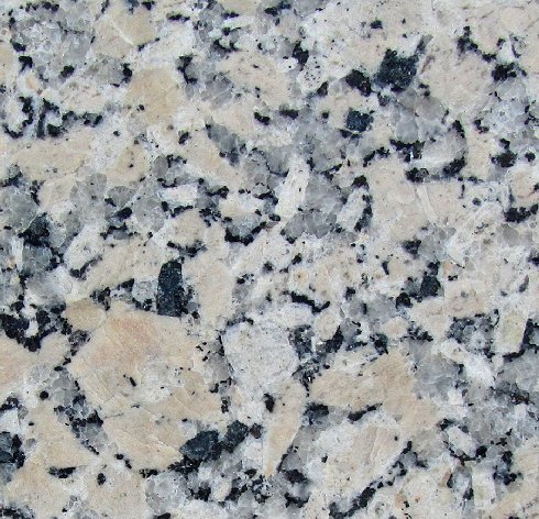
blind as those who will not see. Fine, let me help you. In the following picture you can see a lot of phases and therefore
also phase boundaries between the phases: |
| |
 |
| Phase boundaries in the granite top of my kitchen counter |
|
|
 |
Granite is always a mixture of quartz
(SiO2) and some feldspar (silicates like (KAlSi3O8, NaAlSi3O8,
CaAl2Si2O8, and many more) and, in this particular granite, some mica
(the black stuff; rather complex sheet silicates, e.g. KAl2[AlSi3O10(OH)2]
or muscovite). So we have at least three phases mixed rather haphazardly. |
| |
The
boundary between the melt and a growing (or melting) crystal also constitutes a phase boundary, so you have seen phase
boundaries whenever you have an ice cube in your whisky.
Your skin (loosely speaking) is a phase boundary. On one side
is air, on the other side is you (in the form of bones and some slimy stuff).
More to the point, the boundary between
a crystal of type A (for example pure bcc iron) and a crystal of type B (for example an iron carbide particle) is a phase
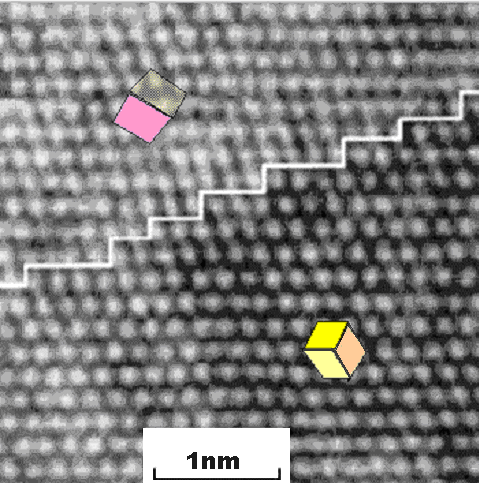
boundary and so is the boundary between bcc iron and fcc iron that is shown below: |
| |
|
|
| |
 |
The white line shows the position of the phase boundary and the insets show schematically
the orientation of the cubic elementary cells. The white dots are columns of iron atoms. |
| |
 |
| Phase boundaries standing "edge-on" |
| Source: Me |
|
|
 |
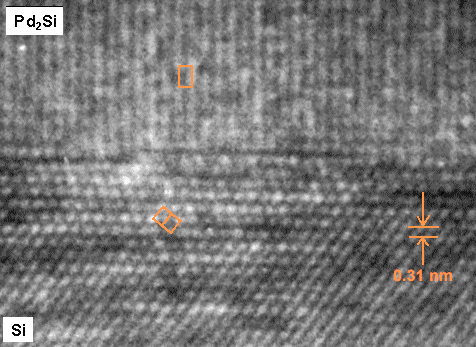
This HRTEM picture shows a phase boundary between fcc silicon (Si) and hexagonal palladium
silicide (Pd2Si). The white dots, just about recognizable, are columns of atoms once more. |
 |
I admit that the phase boundary between fcc silicon (Si) and hexagonal palladium
silicide (Pd2Si) might appear a bit out of phase here. Silicides from one of those
material classes that you have never encountered before and are not important for swords. Nevertheless. they are are quite
important, e.g. for micro electronics. |
|
 |
Chances are that you, personally, are a also direct user of a silicide without knowing that
(hint: look for "molybdenum silicide" in the Net).
Be that as it may, I just happen to like the Pd2Si picture a lot. First, because to the best
of my knowledge, it is the very first high-resolution TEM picture of a phase boundary
ever taken, second, because it was taken by me in 1980. |
 |
So, now you have seen two pictures of actual phase boundaries
at atomic resolution. Or have you? Looking at two-dimensional things only edge-on is
a bit deceiving. Here is an example that needs no further comment: |
| |
 |
 |
Edge-on view and top view of one of ny rug
Since you asked: It is a (modern version of ) a Sivas Sal |
|
|
 |
You are going to miss something for sure, if you look at planar defects only edge-on! |
 |
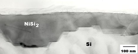
So let's look at some phase boundary in both views, too. I take
some of my own pictures since I don't have to worry about copyright problems then. |
|
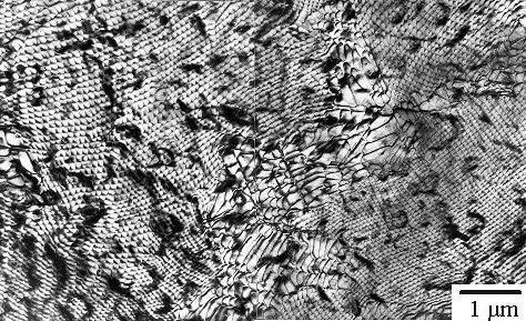
 | |
 | Edge-on view and top view of a phase boundary between
silicon (Si) and nickel silicide (NiSi2) |
|
|
 |
Wow! In the bottom picture a dense network of misfit
dislocations is present. There certainly is a lot to see in the top view that
you don't see edge-on! What you see is even more complicated than in the case of the
grain boundary structure, and you really don't want to know about this.
You do? Good. Maybe you have a feeling that the detailed structure of phase boundaries could be important?
Boy are
you right! Pretty much all of semiconductor technology and in particular optoelectronics
relies on phase boundary engineering. Turn to this advanced
module after you have finished chapter 5. |
|
 |
What the picture also shows in a visual if qualitative way is that phase boundaries are high-energy
defects, just like grain boundaries. We just learned this but it is good to repeat
it.
It should be clear by now that the crystal doesn't want phase boundaries any
more than it wants grain boundaries. However, while it could get rid of grain boundaries in principle if not in practice,
it cannot get rid of phase boundaries as long as it wants to have precipitates
(meaning a completely enclosed second phase; look a chapter ahead if you don't
know what that means) for nirvana reasons. In certain conditions the crystal needs to
have precipitates for achieving nirvana; we will learn about that presently.
The crystal now faces the classical problem
that you can't have your cake and eat it. It can't have precipitates without having
phase boundaries that envelop the precipitates. All it can do is to optimize the situation and that calls for having just
a few large precipitates. All we can do in metal technology is to interfere with the
this optimization process and coerce the crystal to do it in a way we like.
Large precipitates result by the growth
of originally small ones. What that means is that the phase boundary must move—just
like grain boundaries when the grains grow. |
 |
Now back to the topic. You guessed it: in sword making we need to move phase boundaries
around quite a lot too, so we answer the standard question right away: |
| |
Phase boundaries move as soon as
atoms can move around
|
|
|
 |
We have another phenomenon that depends on some diffusion process.
|
 |
The best examples for phase boundaries coming with precipitates are the iron carbide
(Fe3C) particles invariably found inside steel. Whenever they grow or shrink, the phase boundary separating their
surface from the crystal must move. And for doing this, carbon atoms must move, too. |
|
 |
I'm not talking "theory" here but, for example, the making of wootz steel blades where the smith must grow the iron carbide particles to a rather large size.
|
 |
So just accept it. We will encounter phase boundaries a lot when we attempt to
make any sword blade, and they will come up right again in the next paragraph. |
| |
|
© H. Föll (Iron, Steel and Swords script)
