| |
|
 |
We are going to look at phase boundaries in two ways here. First we look at the
general case, after that we consider a very special one. |
|
 |
Dealing with the general case would be quite straight-forward. First, we would acquaint ourselves
in great detail with the science of grain boundaries. We would need far more details
(including a lot of math with matrices and vectors) than what you will find in the link. Then we would add a lot more complexity,
accounting for the fact that the lattices on both sides of the phase boundary are not the same as in the case of a grain
boundary.
If we would do that - and we most certainly will not - all we would find in the end is that the phase boundary
might contain some structures resembling the networks of grain boundary
dislocations, just being more complex. |
 |
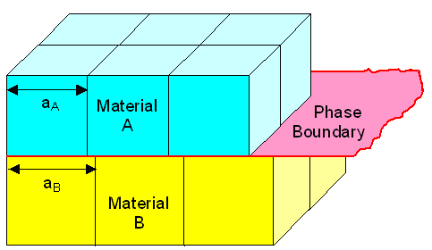
That shall be enough for the general case. Now let's look at a special case of
great importance for technology. For that we consider the most simple phase boundary
imaginable. We will join two crystals of the same kind (cubic, let's say) with no misorientation on a simple plane, for
example on one of the planes of the cube as shown below. |
| |
|
|
|
 |
| The most simple phase boundary imaginable |
|
| |
|
 |
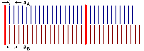
Assuming that the atoms in A and B like each other enough to bond
with gusto, what is going to happen? That becomes clear as soon as we redraw the situation above a bit: |
| | |
|
|
|
 |
 |
 | | Development of misfit dislocations |
|
| | |
|
 |
Since the lattices put on top of each other don't match (top figure), there simply
cannot be a happy atom-by-atom joining across the interphase (note the clever spelling!).
The crystal must do something about this. To understand its options more easily, let's assume that material A is
deposited on top of material B to some small thickness dA. In other words, we are looking
at "thin layer technology", one of the cornerstones of all semiconductor
technology. However, we can make the layer as thick as we like in principle, so all bases are covered here.
There are
exactly two options for the system: substrate B and (thin) layer A: |
|
 |
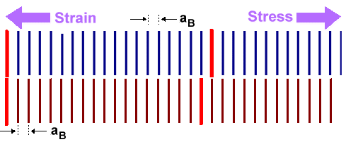
First option: Squeeze one lattice in such a way that it
will match. This is shown in the middle figure. Some stress needs to be applied to the thin layer in this case, producing
the proper strain for matching the lattices. The atoms across the interphase can join now. It is of course the violent mating
of atoms across the interphase that produces the stress; nothing needs to be done from the outside.
There is a price
to pay, however, for all this jolly mating. The upper material in the example is under tensile stress and thus contains
some energy like a wound-up spring. This energy increases directly with the amount of
the misfit and the thickness dA of the layer. |
|
 |
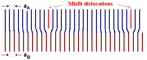
Second option: Introduce misfit
dislocations as shown in the lower figure. In between these dislocations the lattices can be joined by just a little
bending.
Once more there is a price to pay. Dislocations contain energy, and the total cost is proportional to the
total length of the dislocations. Since you need more dislocations to accommodate larger misfit, the price increases with
the amount of the misfit - but is not dependent on the layer thickness dA.
The consequence of this is clear. If the layer thickness is below some critical value dcrit, it
is cheaper to squeeze a bit. If the layer thickness is larger than dcrit, the system is better
off with misfit dislocations. |
 |
We must expect that misfit dislocations are introduced in an interphase as soon
as the critical thickness is surpassed while we deposit the layer. This most certainly (and unfortunately) will happen for
all interphases. Here is just one example (another one can be found in this
link): |
| | |
|
|
|
 |
| Misfit dislocations in the NiSi - Si interphase |
|
| | |
|
|
 |
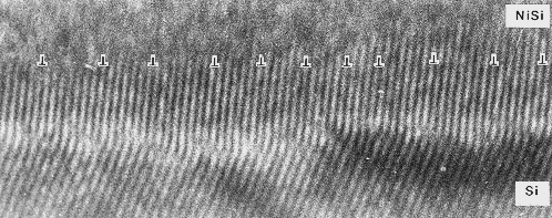
It's a hexagonal NiSi lattice on top of the cubic silicon. No problem, just put the NiSi on
{111} oriented silicon. That's why there is a "kink"
in the lattice planes.
I like this picture a lot because I took it in 1979 and it happens to be the first HRTEM picture showing not only misfit dislocations in a phase
boundary, but the highest density ever encountered by then.
There is a dislocation after about 7 unit cells, which is
a rather high density. In this case an edge-on
HRTEM picture is sensible, because you would not be able to see anything "from the top". The dislocations are
too closely spaced to detect them in any other way. |
 |
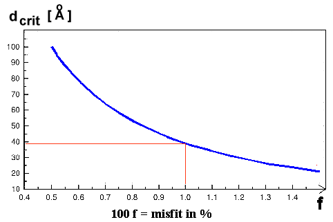
But now let's give the critical thickness dA a closer
look. It is not too difficult to calculate this quantity. The misfit, i.e. the difference in lattice constants, is of importance,
of course, as are the elastic properties of the two materials, i.e. their Young's modulus. In the end a rather simple and
approximate but good equation results that is shown graphically below.
And this equation is really, really bad news: |
| | |
|
|
|
The critical thickness is very small,
even for small misfit
|
|
| | |
|
|
 |
Here is the "master" curve for preventing a lot of good semiconductor products: |
| | |
|
|
|
 |
| Critical thickness as a function of misfit |
|
| | |
|
 |
For a misfit of just 1 %, the critical layer thickness is only about 40 Å
or 4 nm! That is not much. We know a few tricks to enlarge the critical thickness somewhat, but you can't really beat it. |
|
 |
Why is that bad news? Because it means that you cannot make layered structures of various
semiconductors without producing misfit dislocations in the interphases for most cases. And if that happens, your device
is electronically dead. It's that simple.
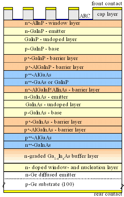
Why would we want make stacks of semiconductors? Because that's what we must
do - otherwise a lot of important devices (like DVD players) would not exist. Let me give you just one example: |
| |
|
| |
|
 |
| World-record solar cell from
2010 | | Layer thicknesses are not to scale. |
|
| | |
|
|
 |
We need to put a hell of a lot of different semiconductors on top of each other to make a
very good solar cell. Same thing for Lasers, LED's, you name it. And most combinations of what we would like to do won't
work because misfit dislocations cannot be avoided!
While the picture above might insinuate that there are plenty of
possibilities left, it is not so. The semiconductors above have been every carefully chosen to do what is wanted of them
as well as possible, while not generating misfit dislocations in the the various interphases. There is a lot of compromising
and long hard work in this structure.
Making much better and simpler solar cells would be possible (and much easier)
if we wouldn't have the misfit dislocation problem. Same thing for Lasers and so on, and for all those gadgets that don't
even exist because of that problem |
 |
One last word. Thanks to oxygen, the atoms on both side of touching materials
do not like to bond. If they would, the interphase formed when you and your partners
skin touch, would not come apart again. Whatever you put on the table would be stuck there. You can easily come up with
the plot for a nice horror movie, assuming that some evil aliens switched off the "do no bond across most interfaces"
law. |
|
 |
Why is that? Because most surfaces already have formed an interface to their oxides. When
you put a silicon wafer on top of another one, they will not easily bond because it is actually a thin layer of silicon
(di)oxide (SiO2) touching another thin layer of SiO2 in just some places (surfaces are usually not
atomically flat ). And all the atoms are thus already quite happy with the (oxygen) partners they have and will not engage
in a little fooling around.
For about the same reason your "skin-oxide" does not bond to that of your partner
and you don't have to worry about misfit dislocations in the skin-skin interphase (about other misfits I don't know).
Fluorine (F) is even better than oxygen to satisfy bonding demands, and that's why nothing sticks to Teflon. |
| | |
|
© H. Föll (Iron, Steel and Swords script)
