 |
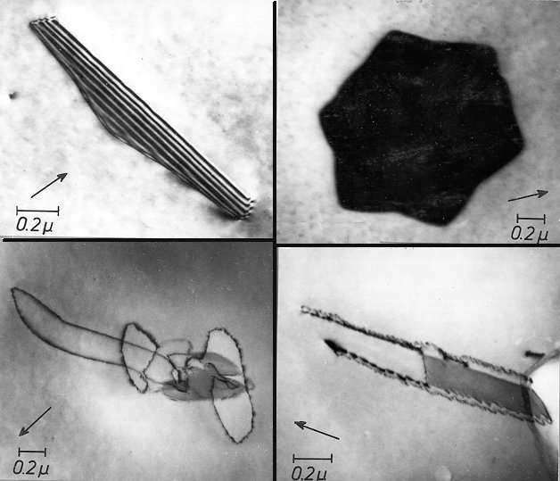
The two top pictures, taken with a transmission electron microscope (TEM),
show simple dislocation loops, bounded by Frank partials, which were generated by the agglomeration of interstitials. The
stacking fault appears with characteristic stripes or at a
brightness different from the background. |
|
 |
The loops are much larger than their equilibrium size - obviously the nucleation of the Shockley partial was not possible; maybe because the Frank dislocation
line is decorated by impurity atoms. |
|
|
|
|
 |
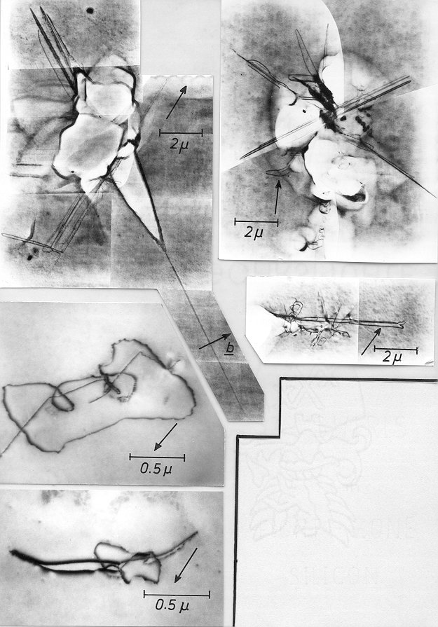
The two pictures above show loop complexes. Some loops still contain stacking faults in parts oft their structures,
but others are perfect and have started to move around. |
 |
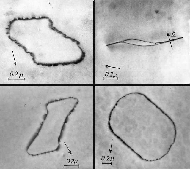
The pictures below show simple loops after the defaulting process. They are now
bound by a perfect dislocation which assumed (more or less) hexagonal shape. |
|
 |
Two segments have started to move way. The "fuzzy" contrast of some dislocations may be due to impurity segregation
or to tiny new Frank loops which nucleated at the dislocation core. This may happen because even after the primary loop
has formed, there are still supersaturated interstitials which tend to agglomerate; but they now find efficient nucleation
sites at the existing dislocations. |
|
|
|
 |
Below are the end products. Complicated dislocation structures have formed; long
dipoles were drawn out at some places. Add a little mechanical stress and you will have a crystal full of dislocations (and
unsuited for integrated circuits). |
|
|
|
© H. Föll (Defects - Script)


![]() Etch Pattern of Swirl Defects in Silicon
Etch Pattern of Swirl Defects in Silicon ![]() 5.4.2 Dislocation Reactions Involving Partial Dislocations
5.4.2 Dislocation Reactions Involving Partial Dislocations ![]() 6.3.3 Stacking Faults and Other Defects
6.3.3 Stacking Faults and Other Defects