 |
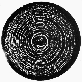
The micrograph shows a 100 mm
Si wafer after preferential etching. The wafer was cut from a large as-grown crystal and only polished before etching.
|
|
 |
The crystal was grown with the float-zone
technique and represented the state of the art in about 1972. The typical spiral pattern of the small etch pits
lead to the name "Swirl defects". These defects were extremely detrimental to the functioning of integrated circuits
and power devices made from the wafer. It was thus of prime importance to learn about their nature so that they could be
avoided. |
|
|
 |
The picture was taken under "dark field" conditions. The wafer is illuminated at
an angle; only light that is scattered at defects reaches the lens of the camera. Perfect areas are totally black. The defects
must be due to agglomerates of the point defects (including perhaps the major impurities O and C) that were
present a high temperatures - presumably in thermal equilibrium. |
 |
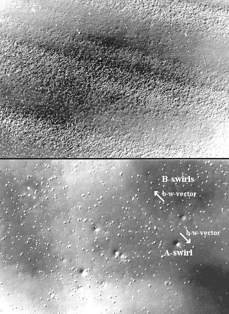
The etch pattern at high magnifications as seen through an optical microscope reveals two types
of defects (see also the pictures in the link) The first picture
is at an intermediate magnification, the second one at high magnification: |
|
|
 |
Lots of small etch pits can be seen in a striated pattern - the swirl pattern. The inner areas
of the wafer may only contain these "B-type" defects, whereas closer to the edge of the wafer, some large
hillocks - the A-type" swirl defects are contained within the B-defects. Hillocks and pits give different
signs of the black-white contrast (the vector from the black part of the contrast to the white part); this serves to distinguish
between the two possibilities. |
 |
The a-type swirl defects are dislocations loops and dislocation loop clusters of interstitial
type - the loops shown before. This result was the first direct
observation that showed that self interstitials play a role in Si. Etching techniques can not provide a result like that. |
|
 |
In fact, it was never possible to establish the nature of the B-type defects. They might be "fore-runners
of the A-type defects - i.e. some kind of interstitial agglomerate - or small vacancy agglomerates; possibly small
voids; but nobody knows for sure. |
|
 |
Since present day crystals are much larger and grown with different techniques, swirl defects are now longer
seen. But other types of defects (called C- and D-defects) are present now and always first detected by optimized
preferential etching solutions. D-defects meanwhile have been identified as small voids, i.e. vacancy agglomerates |
| | |
© H. Föll (Defects - Script)


![]() 6.3.2 Examples and Case Studies for Dislocations
6.3.2 Examples and Case Studies for Dislocations ![]() Generation of Dislocation Structures by Agglomeration of Interstitials in As-Grown Silicon Crystals
Generation of Dislocation Structures by Agglomeration of Interstitials in As-Grown Silicon Crystals