| |
Pictures to: 3.1 TEM Work at Cornell University |
| |
3.1.1. TEM Investigations of Grain Boundaries in Silicon |
| |
Part 2: Fig. 9 - Fig. 16 plus some Auxiliaries |
 |
In what follows I present the pictures used for the one and only major publication concerned with the structure of the grain boundaries. Besides the originals, I give some auxiliary pictures that show essentially
the same structure. |
|
 |
You are going miss Fig. 8 ? Sorry - I have no good print of that picture anymore. |
| | |
|
| |
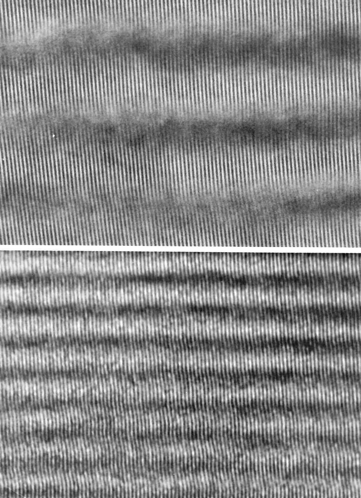 |
Fig. 9 in publication.
(111) lattice fringes across two low-angle boundaries on (100) planes.
Tlted-beam illumination and a specimen orientation close to a (112) pole was used for this and the following lattice-fringe
images. The spacing between the fringes is 0.31nm. |
| I fondly belie that this is the very first high-resolution TEM (HRTEM) picture of screw dislocations. It shows directly the typical
drawings shown in text books |
|
| |
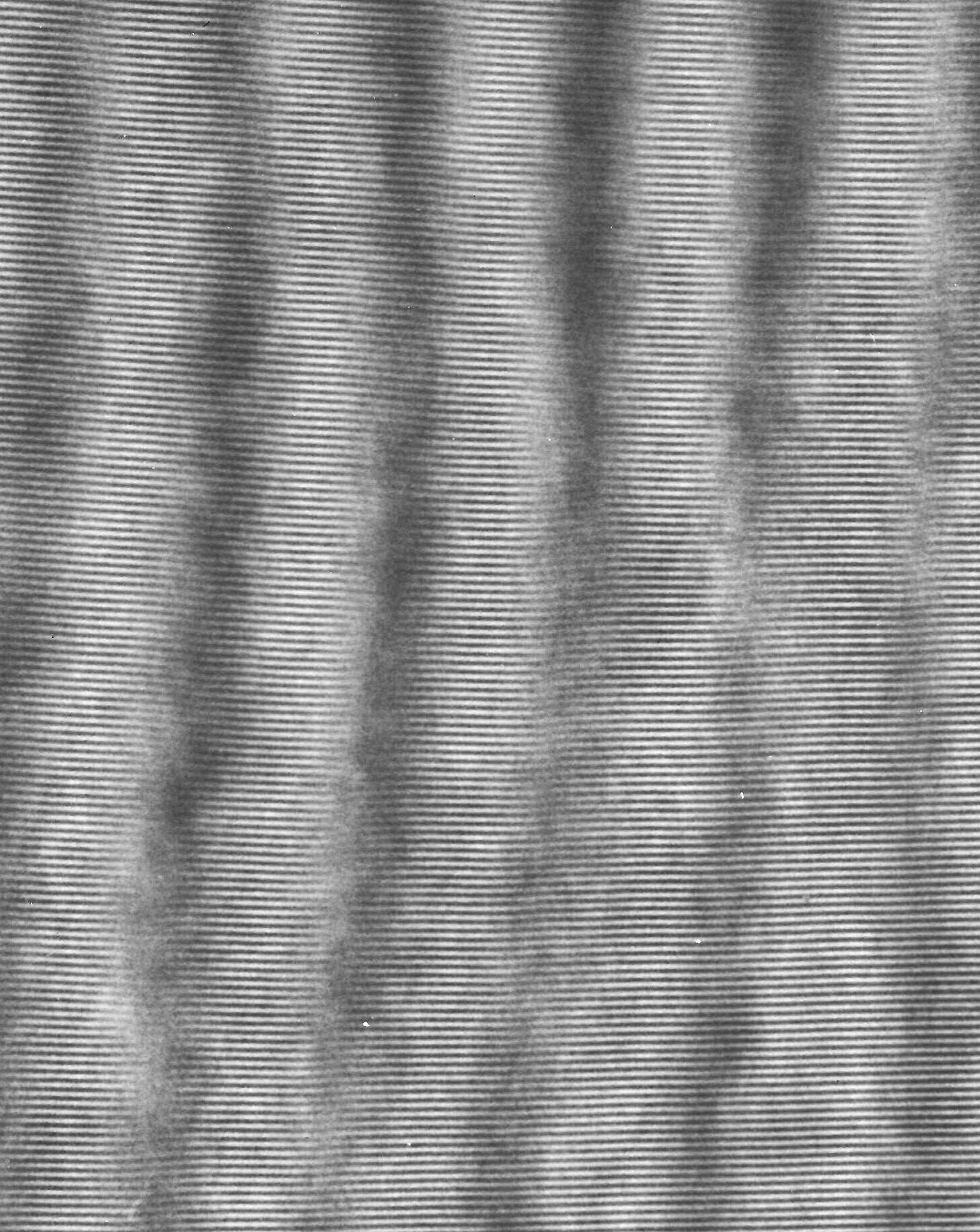 | | Detail rto Fig. 9 |
|
| |
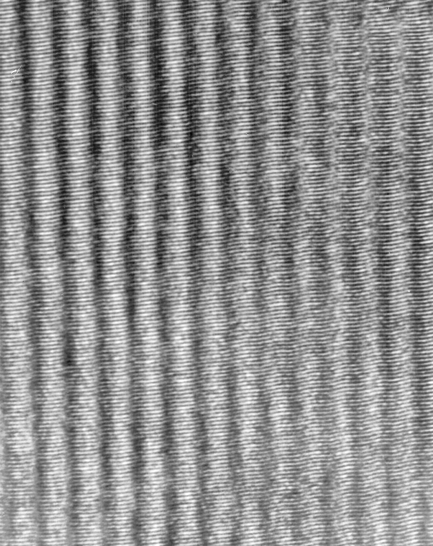 | Detail to Fig. 9
|
|
| |
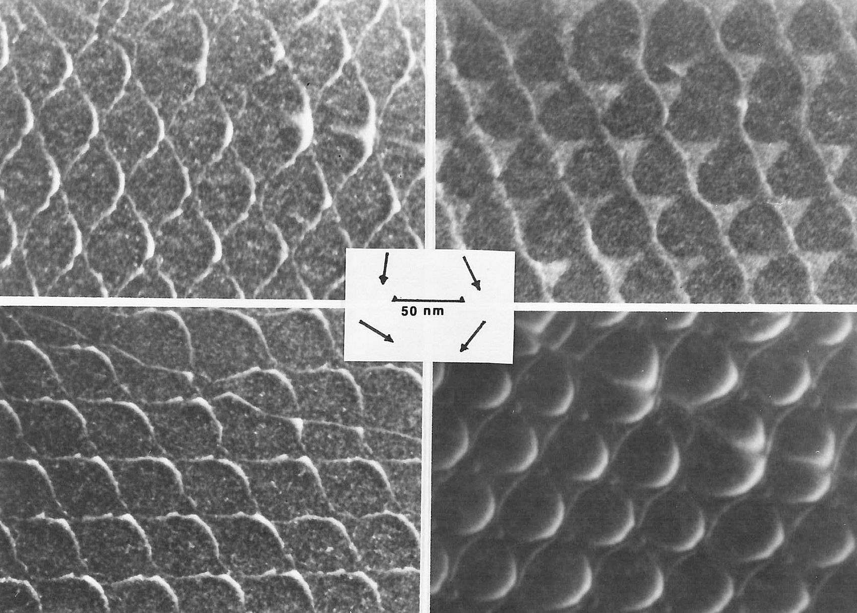 |
| Fig. 10 in publication. |
|
| |
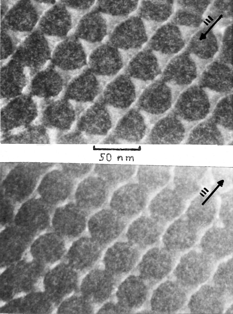 |
Relating to Fig. 10.
Showing contrast change from intrinsic to extrinsic stacking
fault
upon changing the sign of the diffraction vector |
|
| |

| . Relating to Fig. 10 in publication; as above
|
|
| |
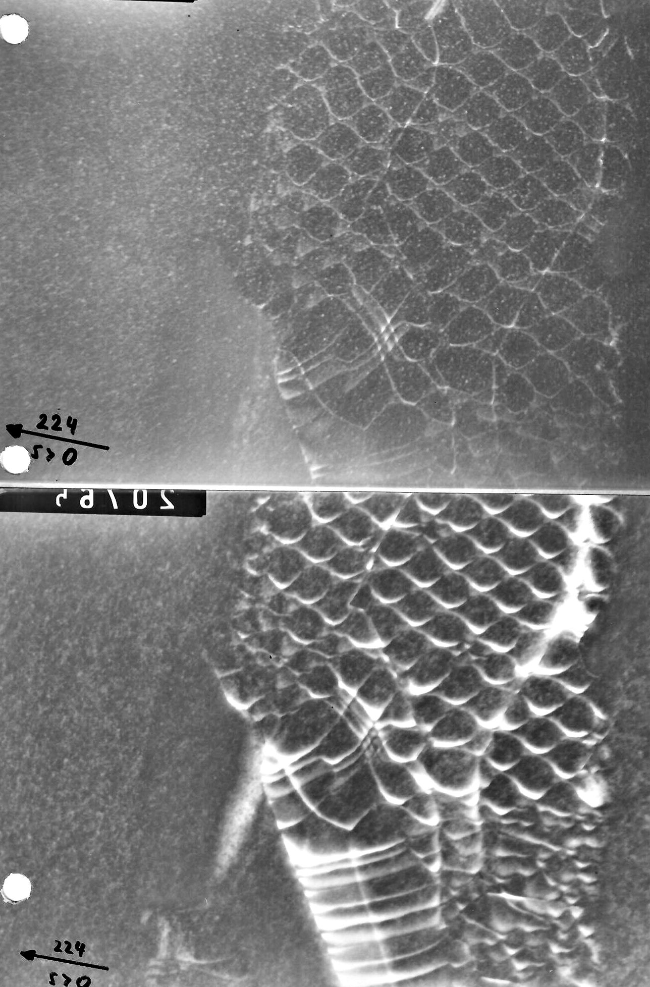 |
Auxiliary picture to Fig. 10.
Increasing the excitation error in weak beam increases resolution
but decreases contrast.
It also needs longer exposure times and thus increases the risque of blurring |
|
| |
| | Fig. 11 in publication. |
| Weak-beam and lattice-fringe image of a low-angle twist boundary on a (111) plane. |
|
| |
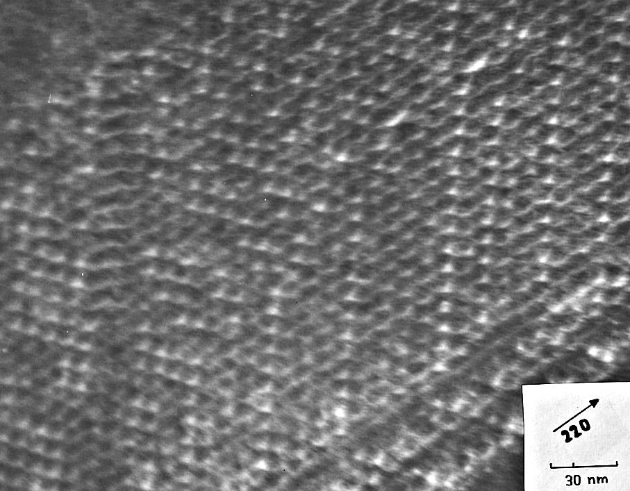
| | Detail to Fig. 11. |
|
| |
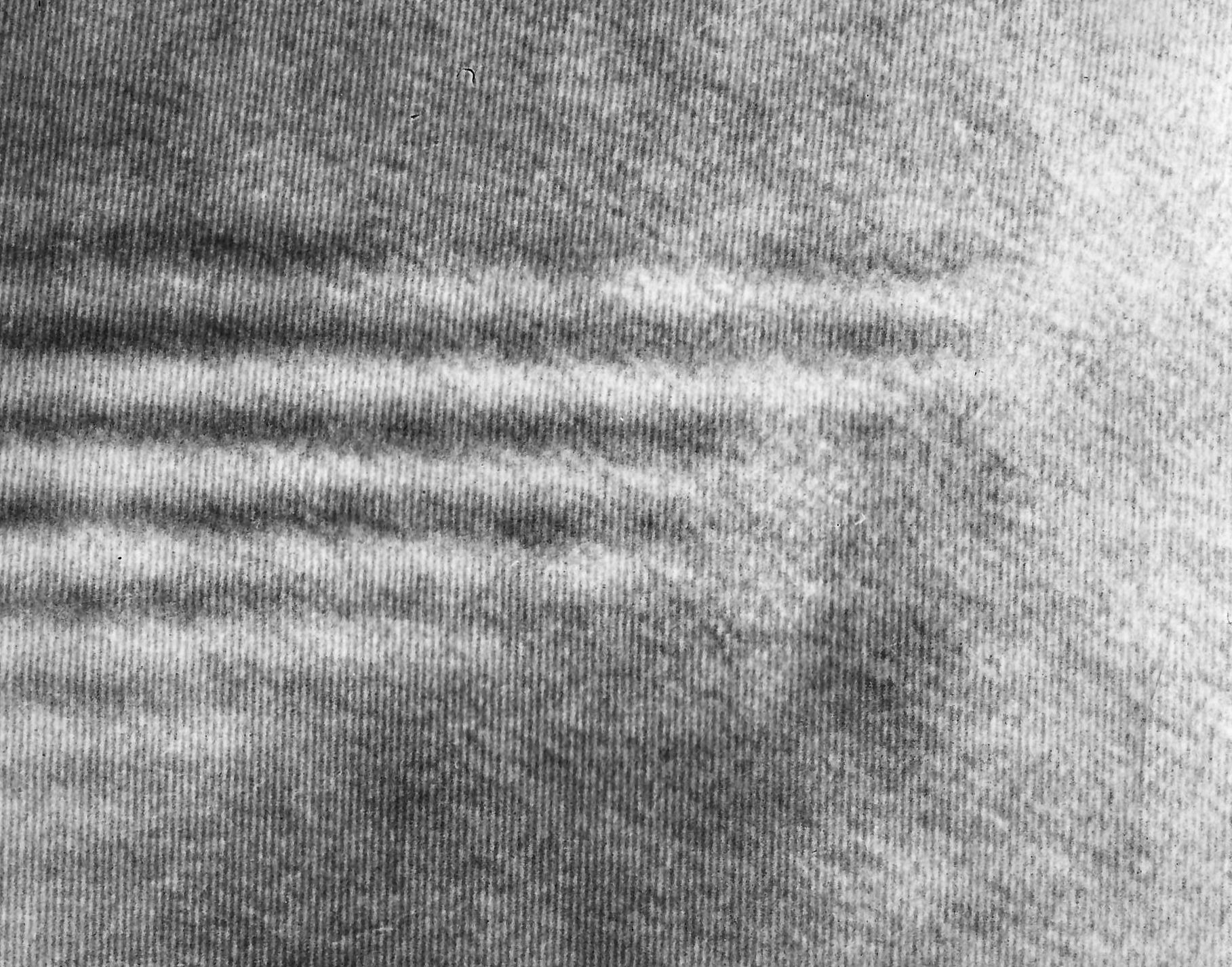
| | Fig. 12a in publication. |
| Low-angle twist boundary on a (111) plane imaged with two different sets of (111) lattice fringes. |
|
| |
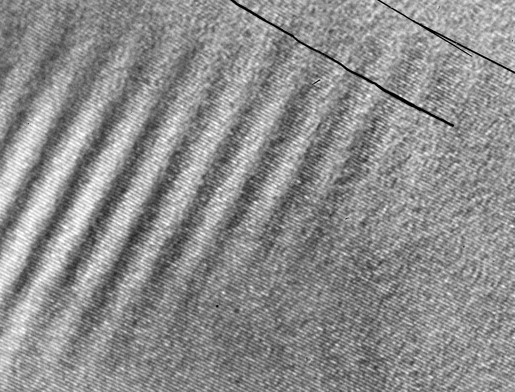
| | Fig. 12b in publication. |
|
| |
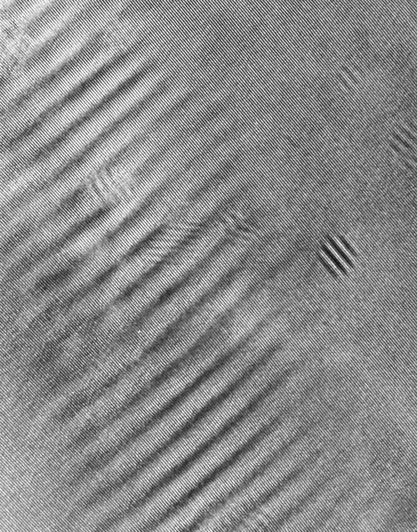
| | Relating to Fig. 11 / 12 in publication to Fig. 6 in publication. |
|
| |
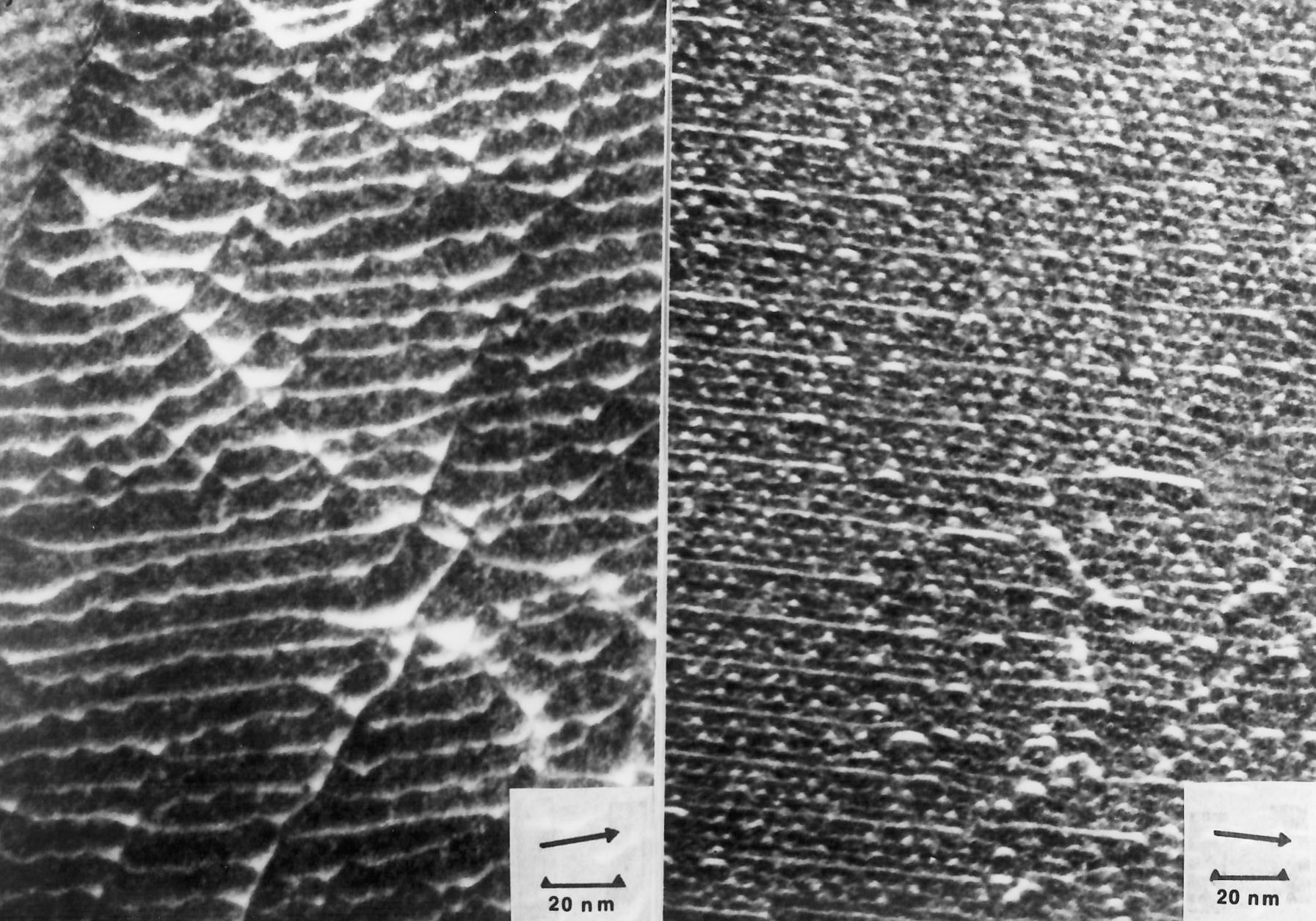
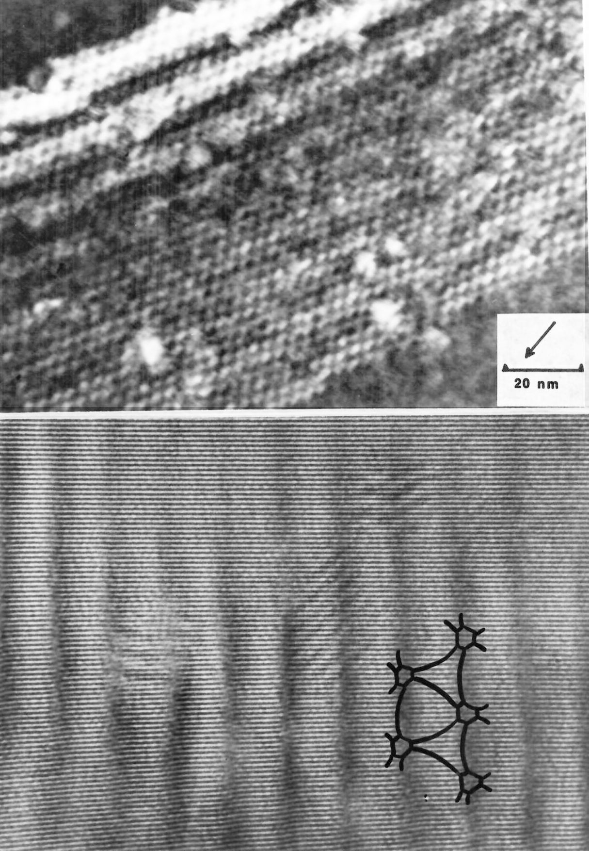
| | Fig. 13 in publication. |
|
| |
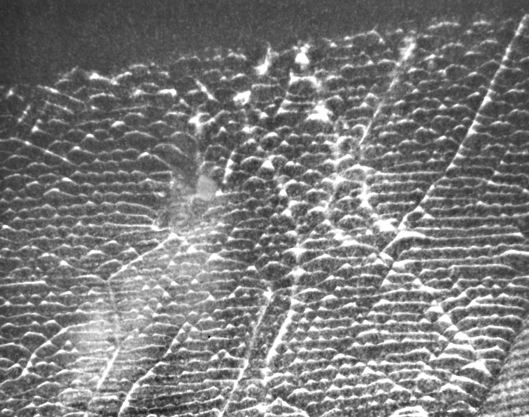
| | Similar to Fig. 13. |
|
| |
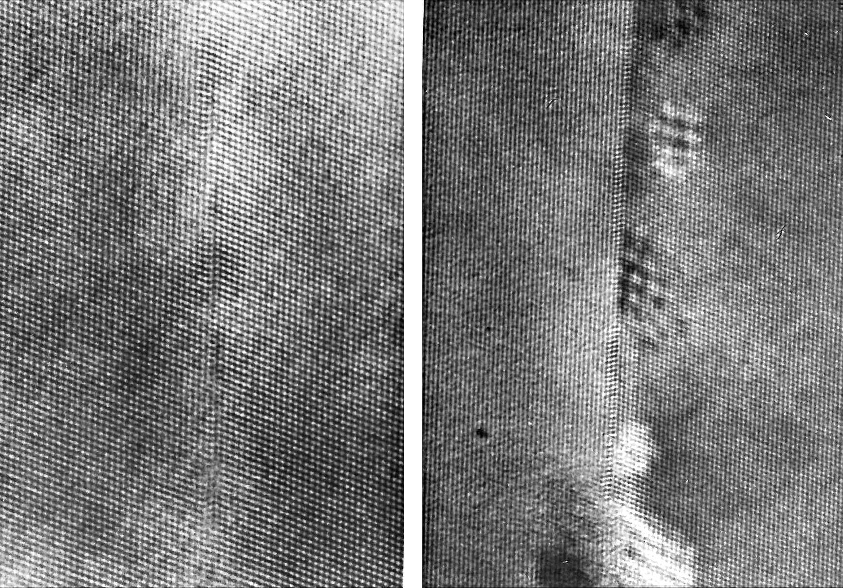
| | Fig. 14 in publication. |
|
| |
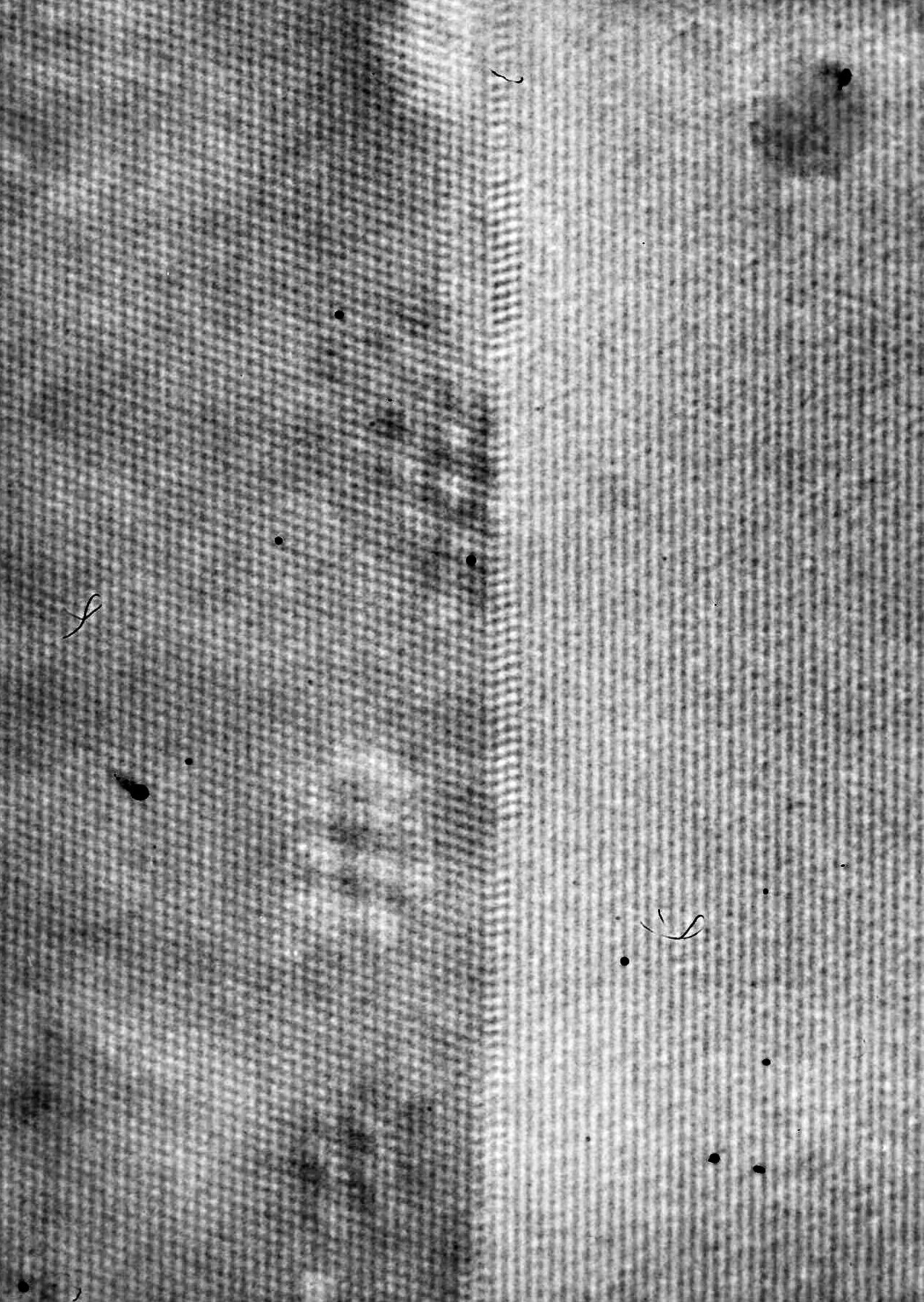 | | Other view of part of Fig. 14. |
|
| |
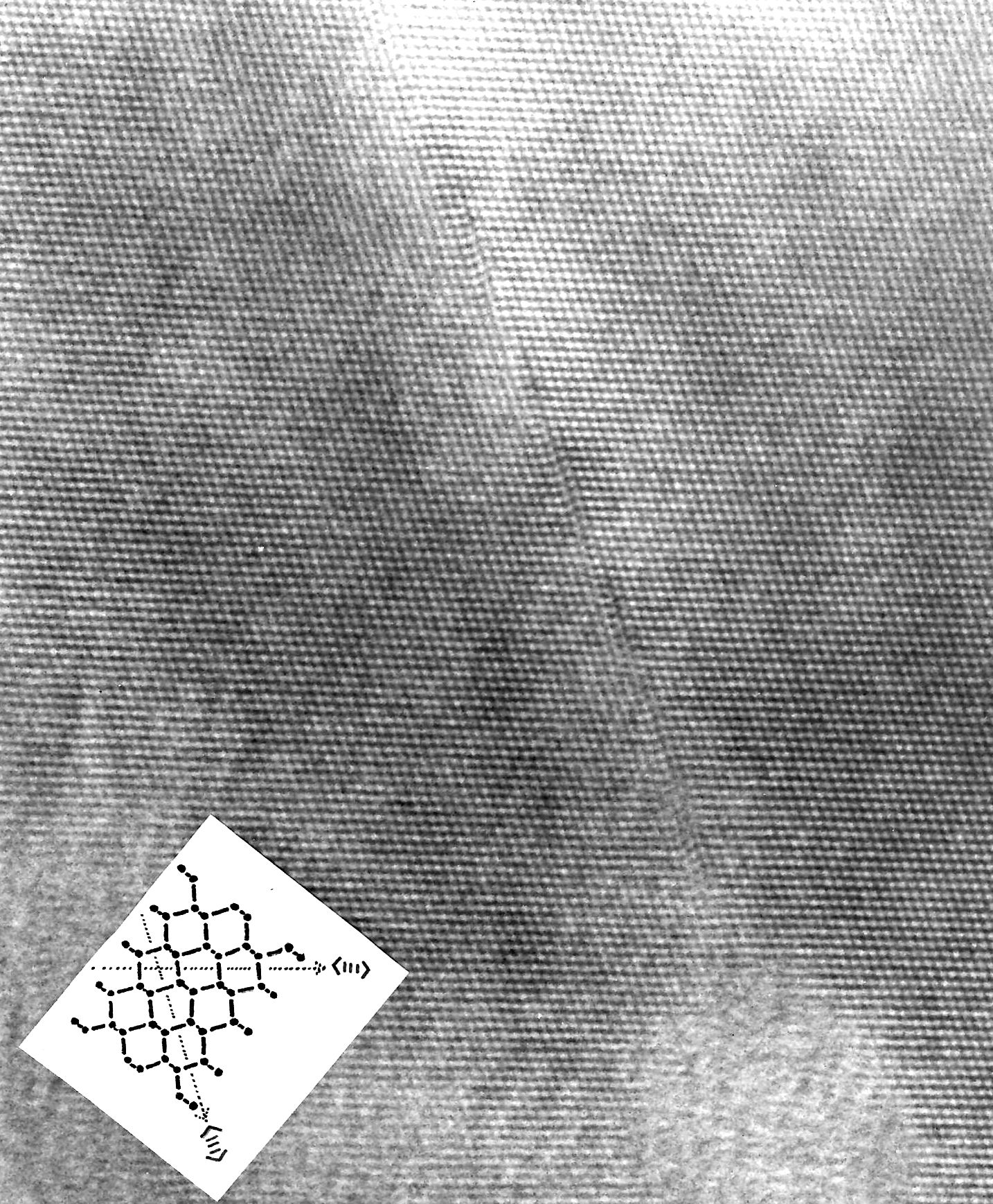 | | Part of Fig. 14. |
|
| |
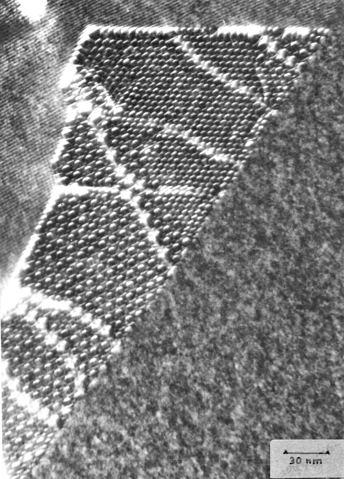
| | Close to Fig. 15 in publication. |
| Low-angle twist boundary on a (111) plane imaged with g=(224) exhibiting the structure of 8 twin boundary
in the right-hand side |
|
| |
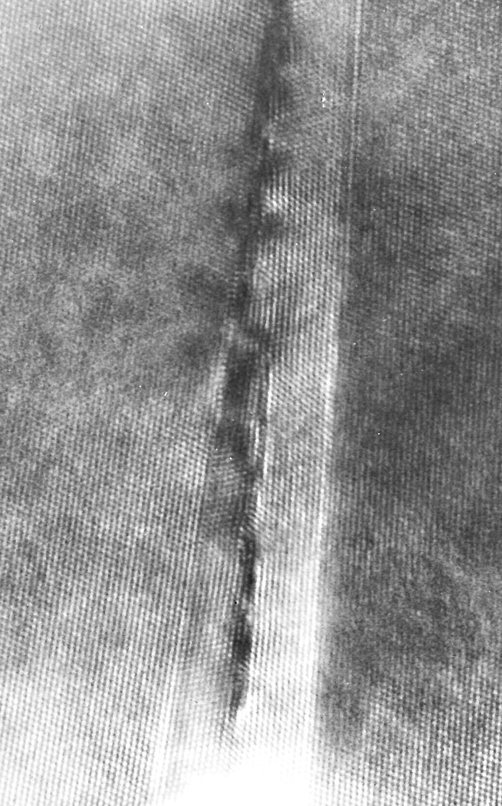
| | Fig. 16 in publication. |
| Direct lattice image of a low-angle twist boundary on a {llI} plane with an additional tilt component split
into twin boundary |
|
| |
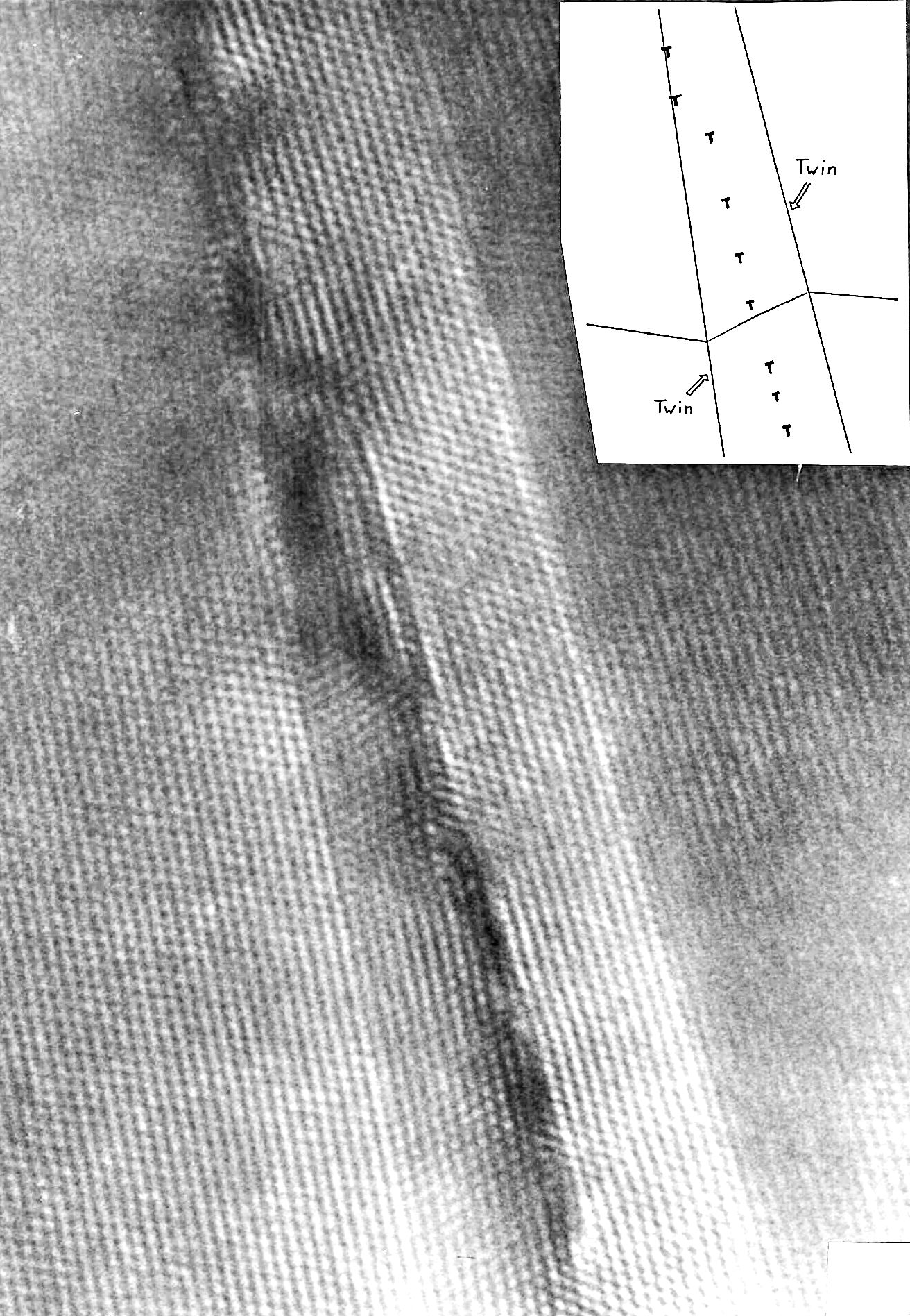 | | Fig. 16b once more. |
|
 With frame

 3.1 TEM Work at Cornell University; 3.1 TEM Investigations of Grain Boundaries in Silicon
 Pictures to: 3. TEM Work at Cornell University; 3.1.1. TEM Investigations of Grain Boudnaries in Silicon
 Pictures to: 3.1 TEM Work at Cornell University; 3.1.1. TEM Investigations of Grain Boundaries in Silicon
© H. Föll (Archive H. Föll)
![]() 3.1 TEM Work at Cornell University; 3.1 TEM Investigations of Grain Boundaries in Silicon
3.1 TEM Work at Cornell University; 3.1 TEM Investigations of Grain Boundaries in Silicon