| |
Pictures to: 3. TEM Work at Cornell University |
| |
3.1.1. TEM Investigations of Grain Boudnaries in Silicon |
 |
In what follows I present the pictures used for the one and only major publication concerned with the structure of the grain boundaries. Besides the originals, I give some auxiliary pictures that show essentially
the same structure. |
| |
|
|
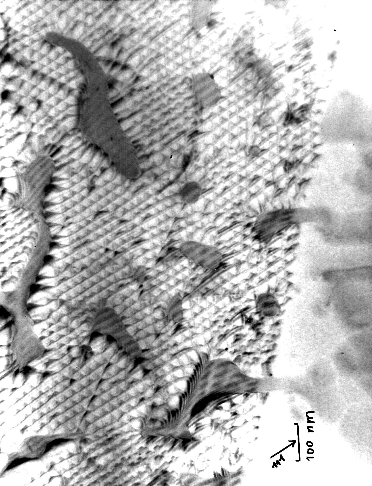
| | Fig. 2 in publication. |
| Kinematical bright-field image of a low-angle twist boundary on a (111) plane. The diffraction vector in
this and the forthcoming figures is indicated by narrow; here it is g = {lll}. |
|
| |
|
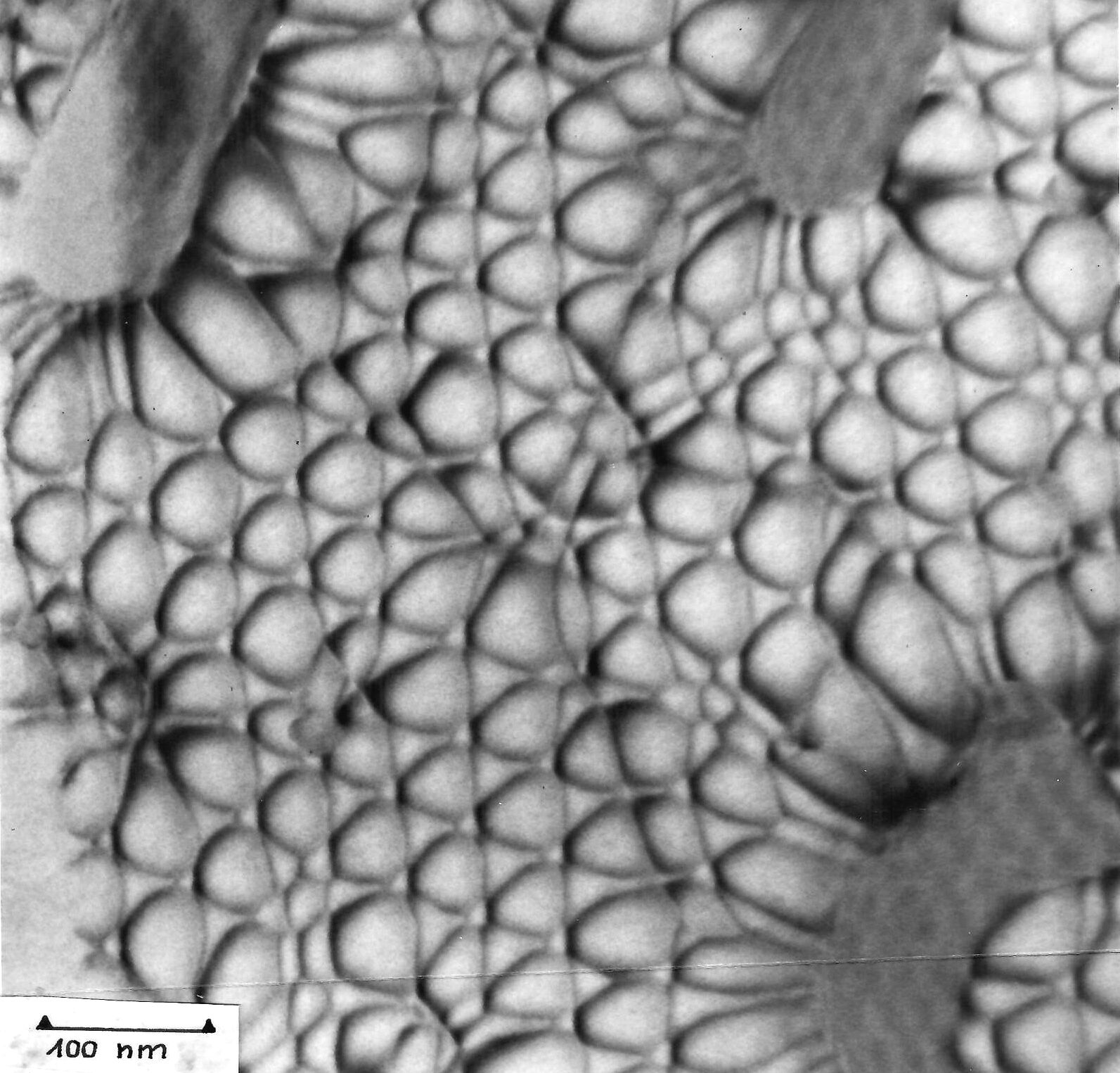
Auxiliary picture to Fig. 2 in publication.
Different contrast conditions show the complete
network and the stacking faults in the knots |
|
| |
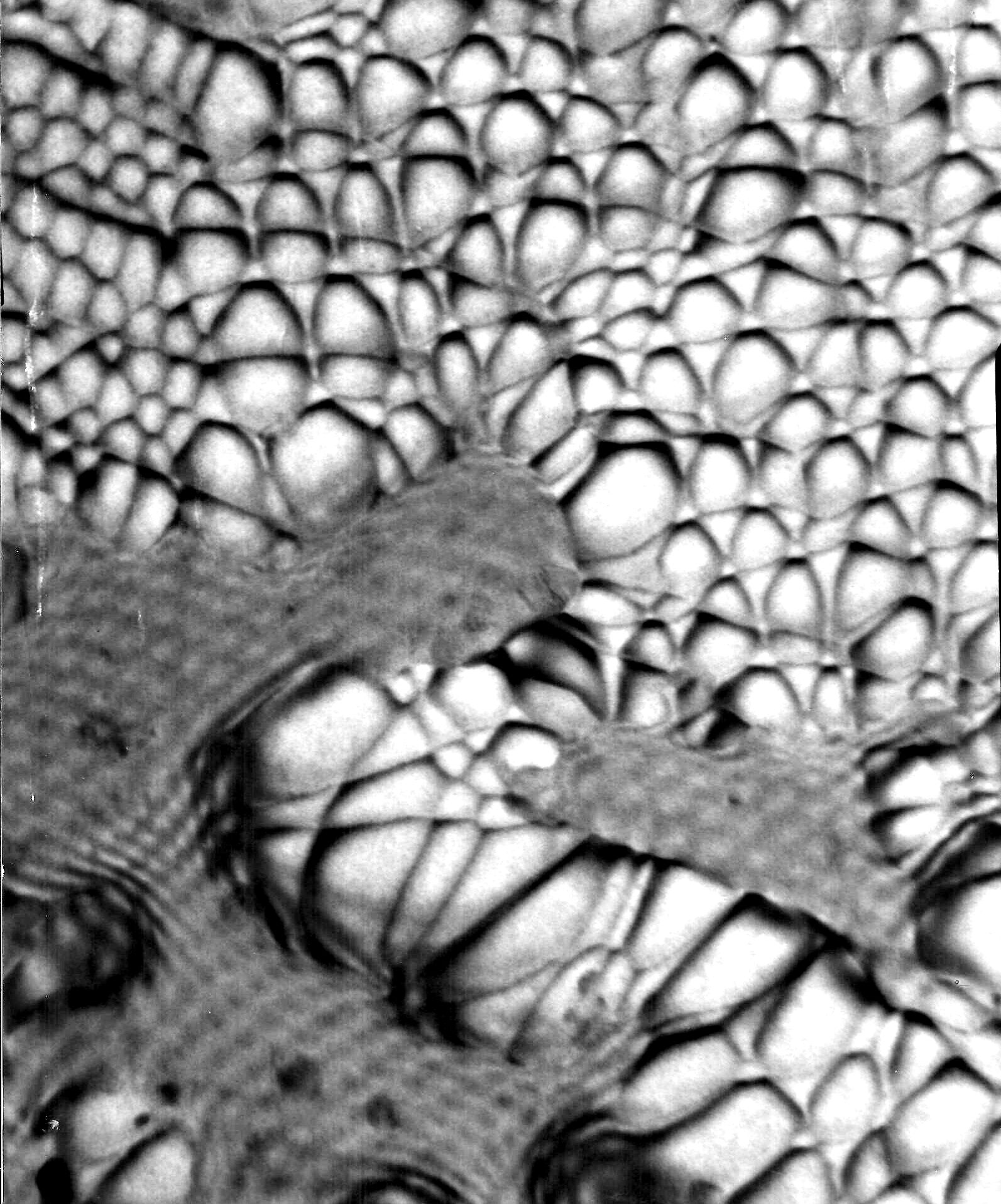
| Same as above.
On the upper left the network switches to the simple heaxagonal form in a twin boundary |
|
| |
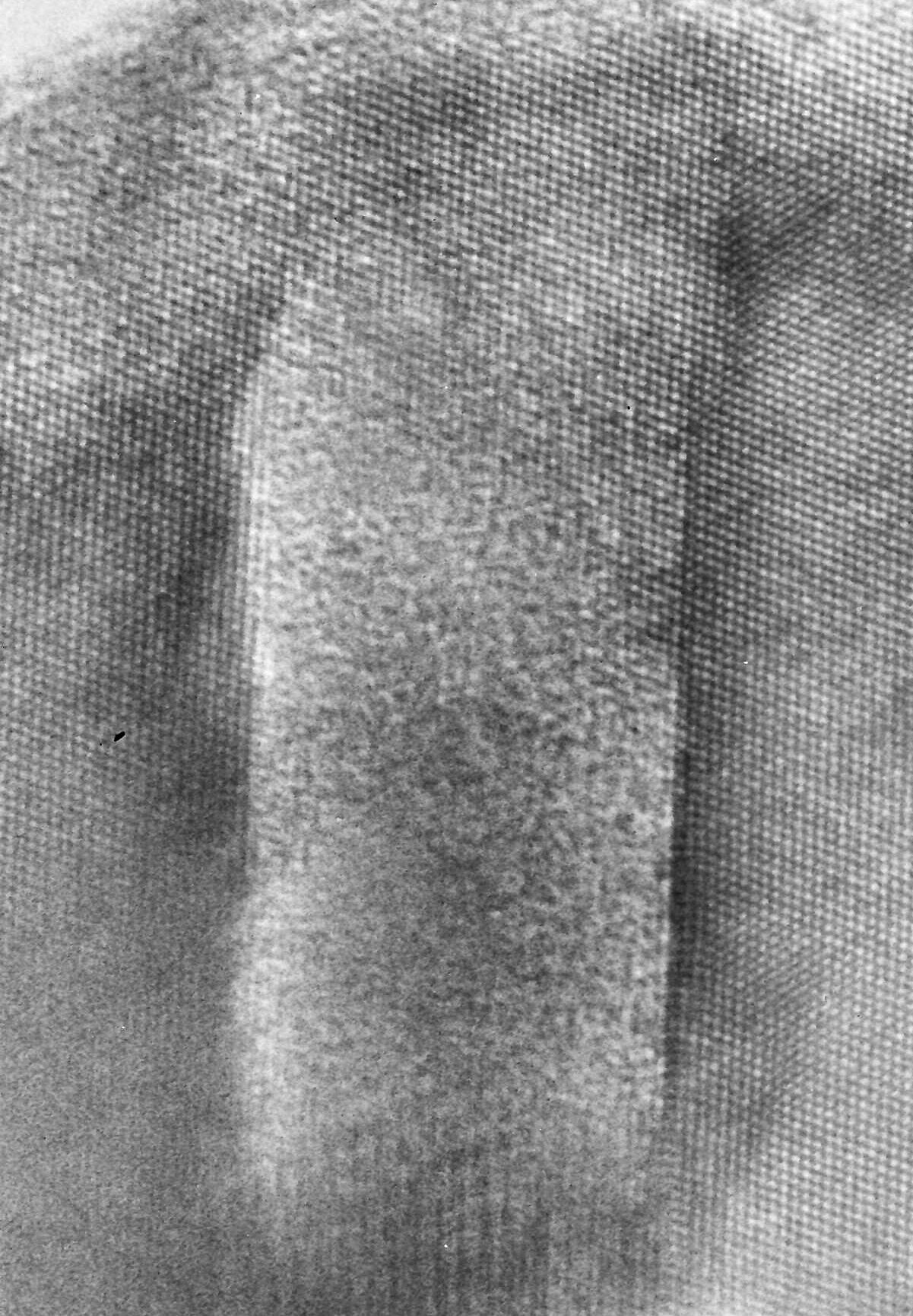 |
| Fig. 3 in publication. |
| Direct lattice image of an amorphous region. White ' dots ' can be thought to correspond to the open channels
in a <110> direction; the spacing of the fringes is 0.31 nm . |
|
| |
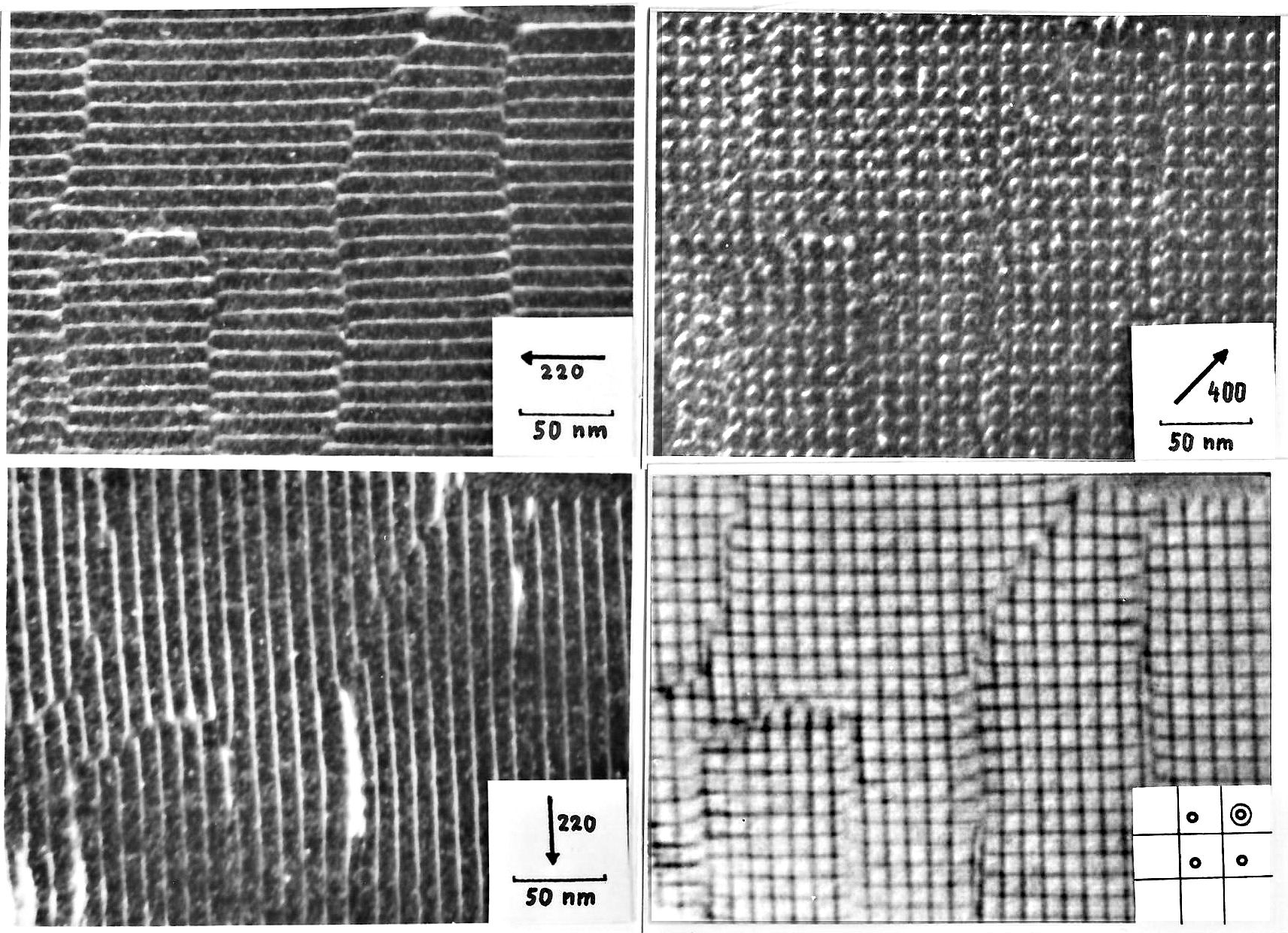
| | Fig. 4 in publication. |
| Low-angle twist boundary on a (100) plane imaged with different diffraction conditions. g={220) in 4 (a,c);
g=(400) in 4 (b ); 4 (d) was taken with multi-beam conditions close to the (100) pole. The (220) Kikuchi bands, the major
diffraction spots end the position of the aperture on the primary beam are indicated. |
|
| |
|
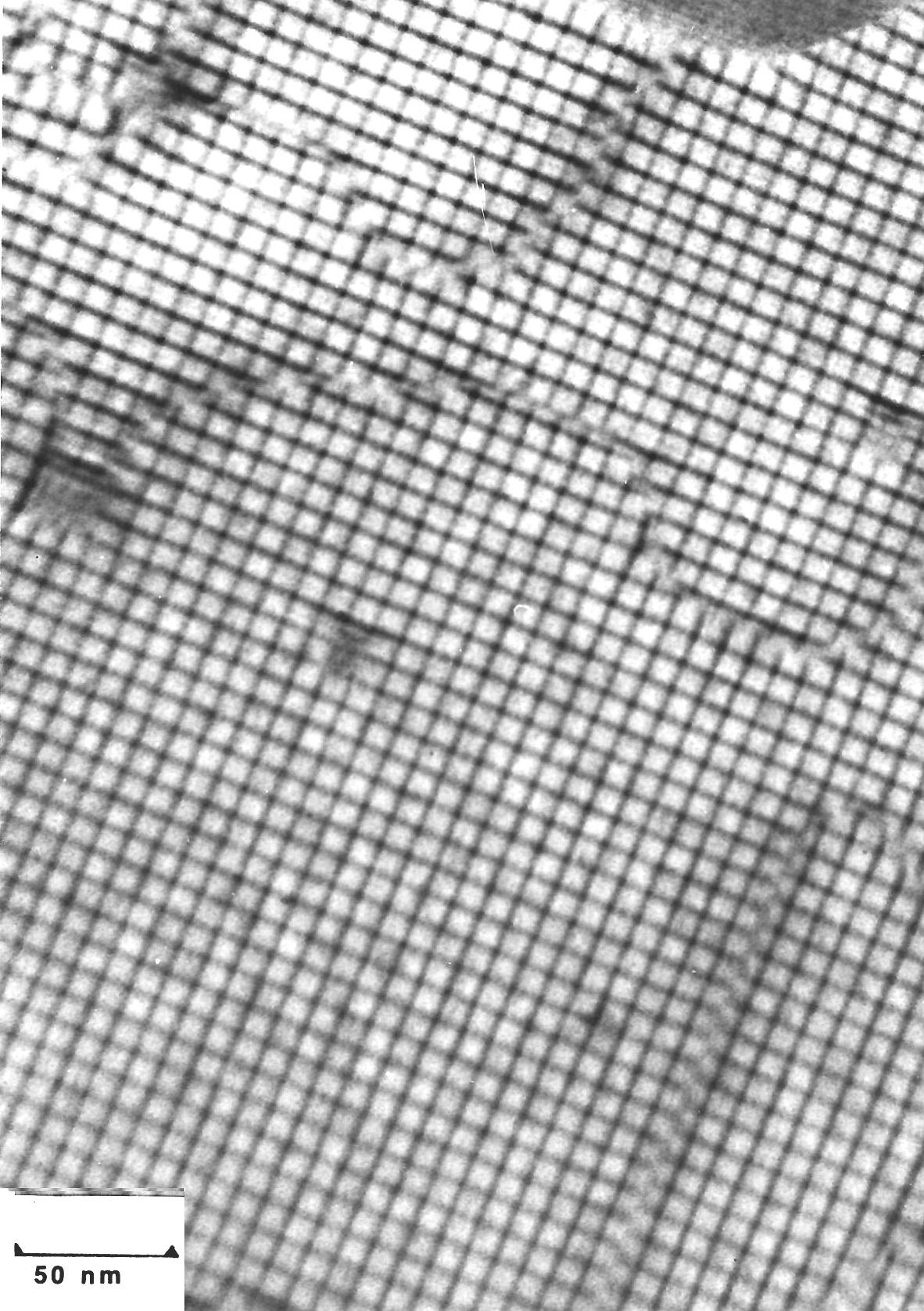
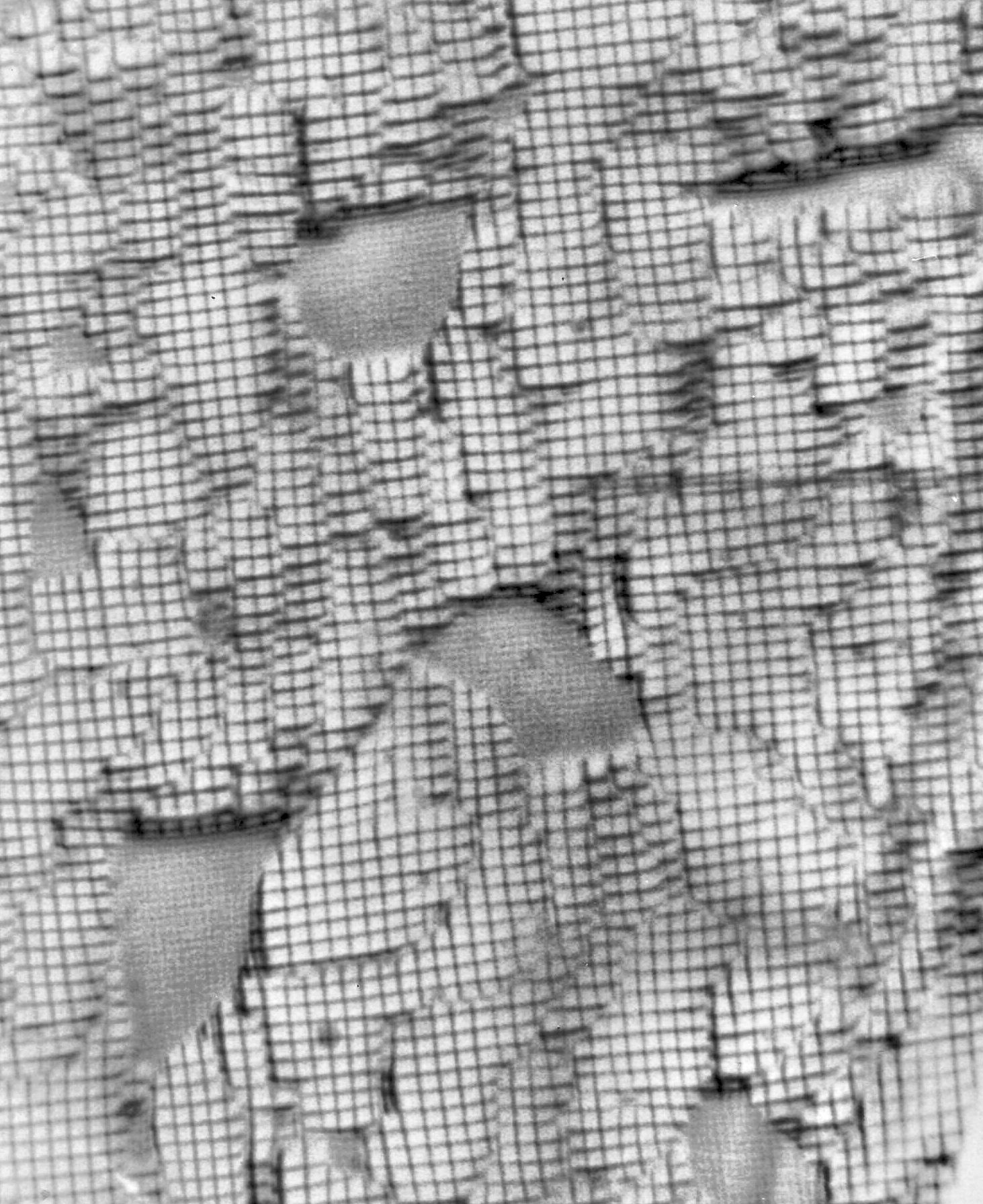
Fig. 6 in publication
The "famous" picture showing the "text book" structure
of as low-angle twist boundary on
a {100 plane} with its square network of screw dislocations. |
| |
|
| |
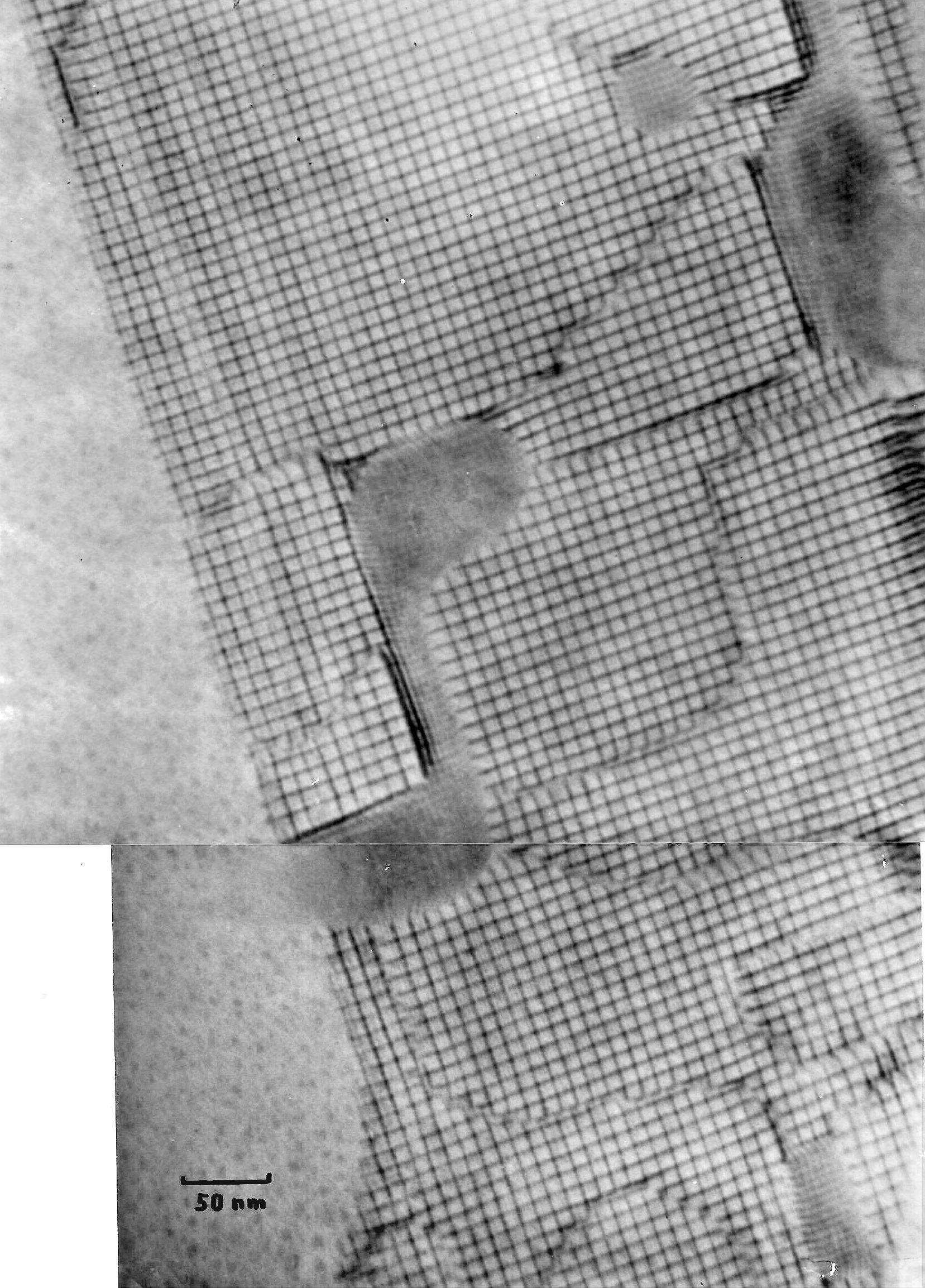
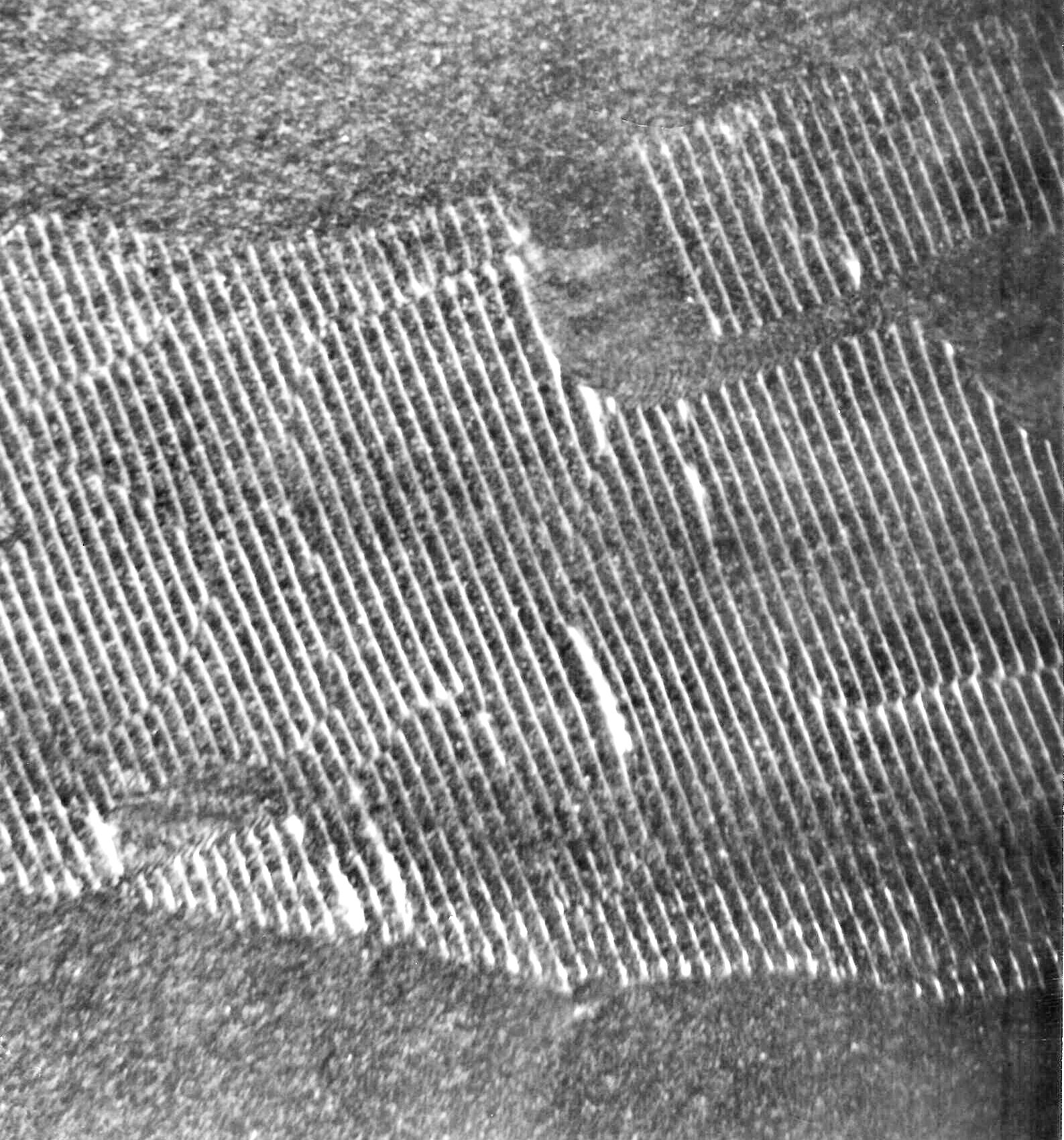
| | Auxiliary picture to Fig. 6. |
| Extrinsic dislocations in the dislocation network of a low-angle twist boundary on a (100) plane.
|
|
| |
|
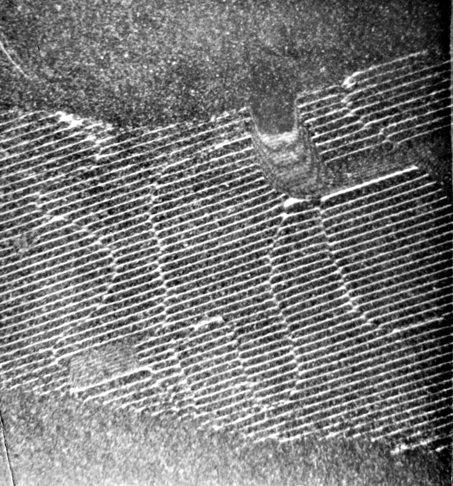
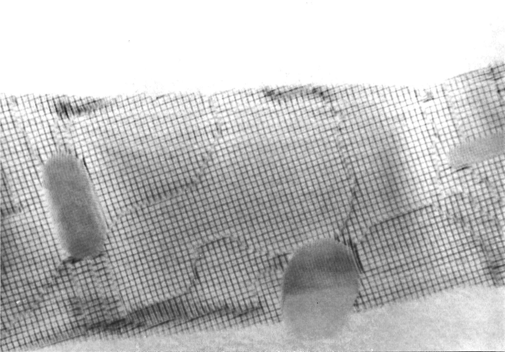
| Part of the structure shown above. Weak beam, showing only one set of dislocations. |
|
| |
|
| Complementary picture to the one above. Showing the other set of screw dislocations. |
|
| |
| | Similar to Fig. 6 in publication. |
|
| |
| | Similar to Fig. 6 in publication. |
|
| |
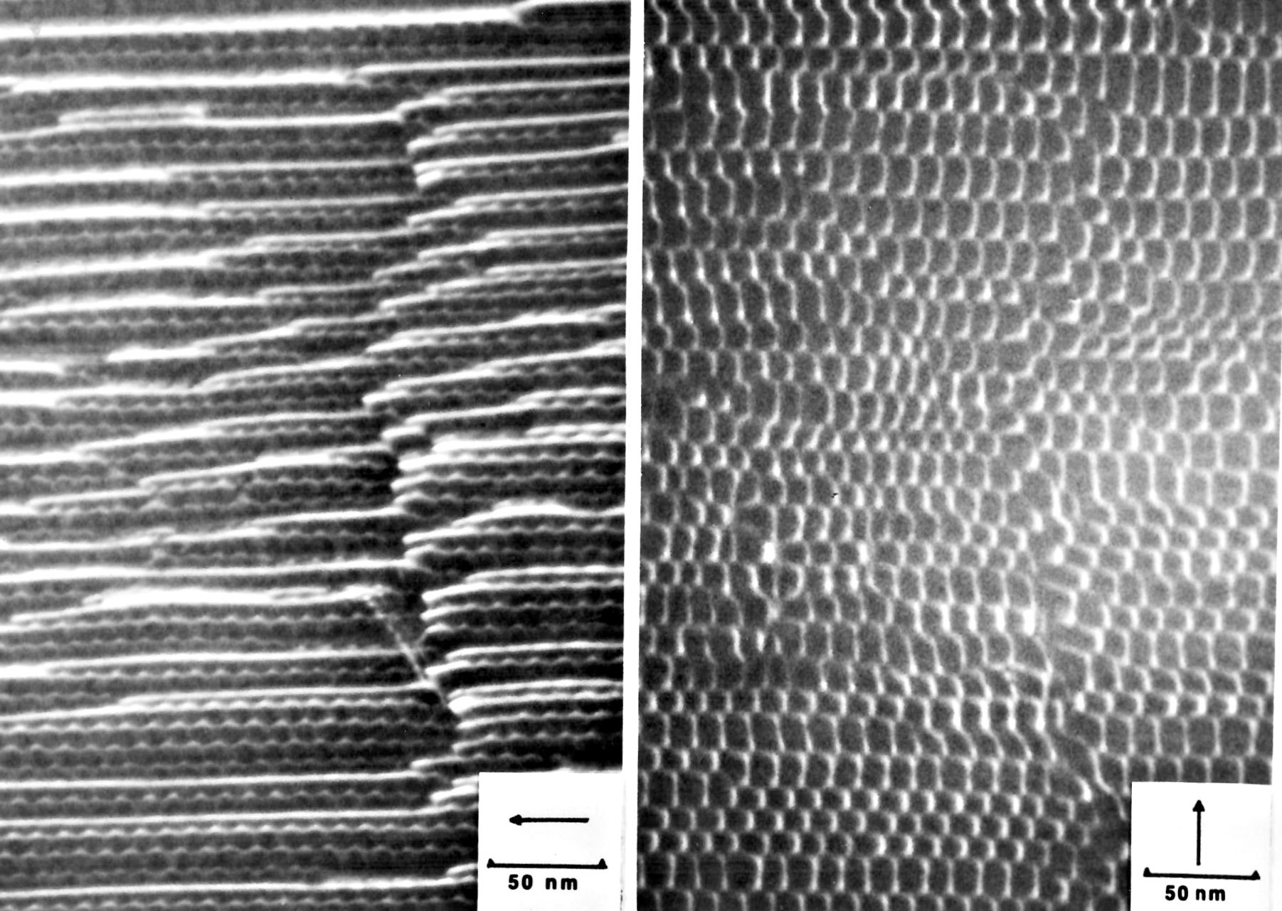
| | Fig. 7 in paper. |
|
| |
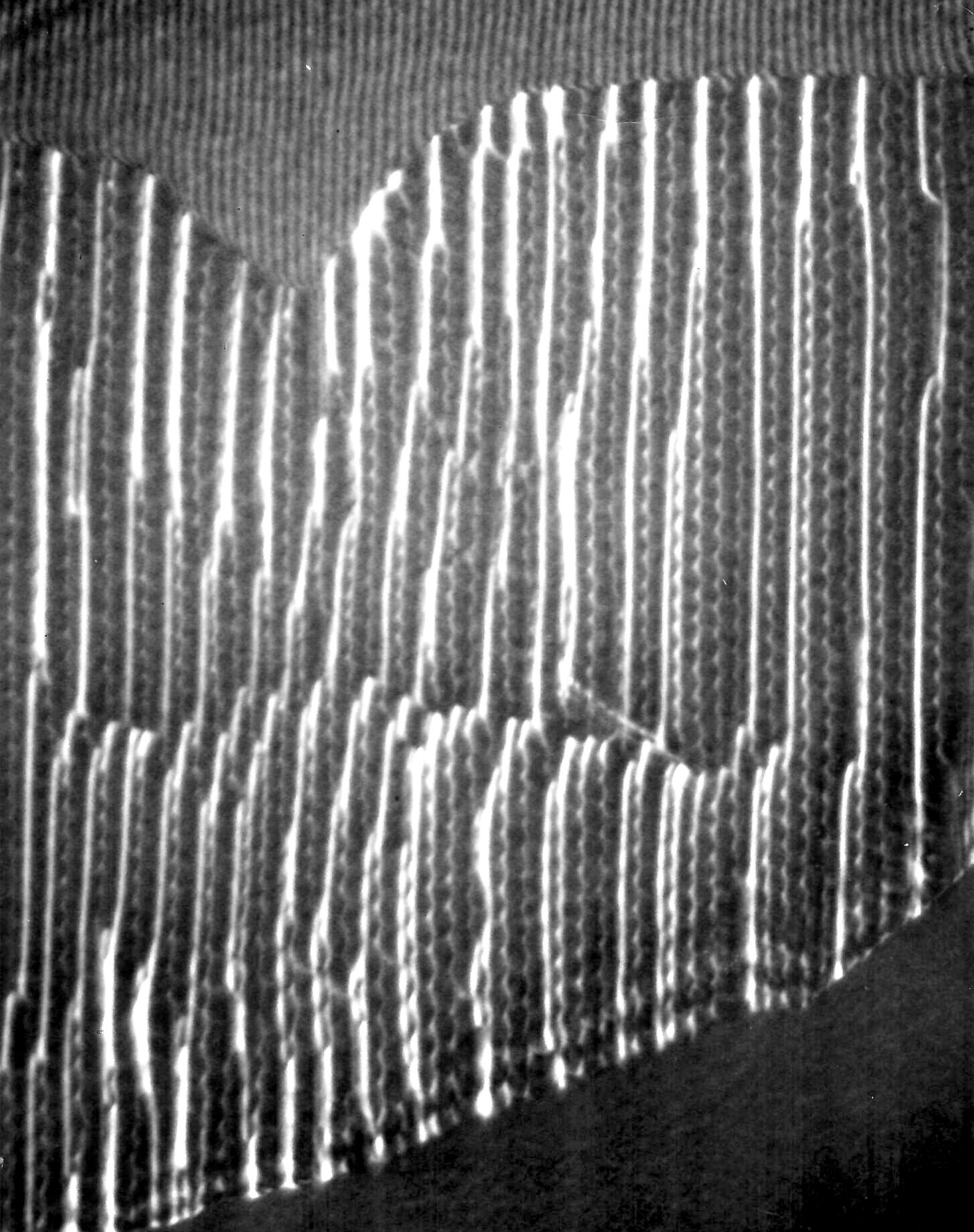
| | Detail of Fig. 7. |
|
| |
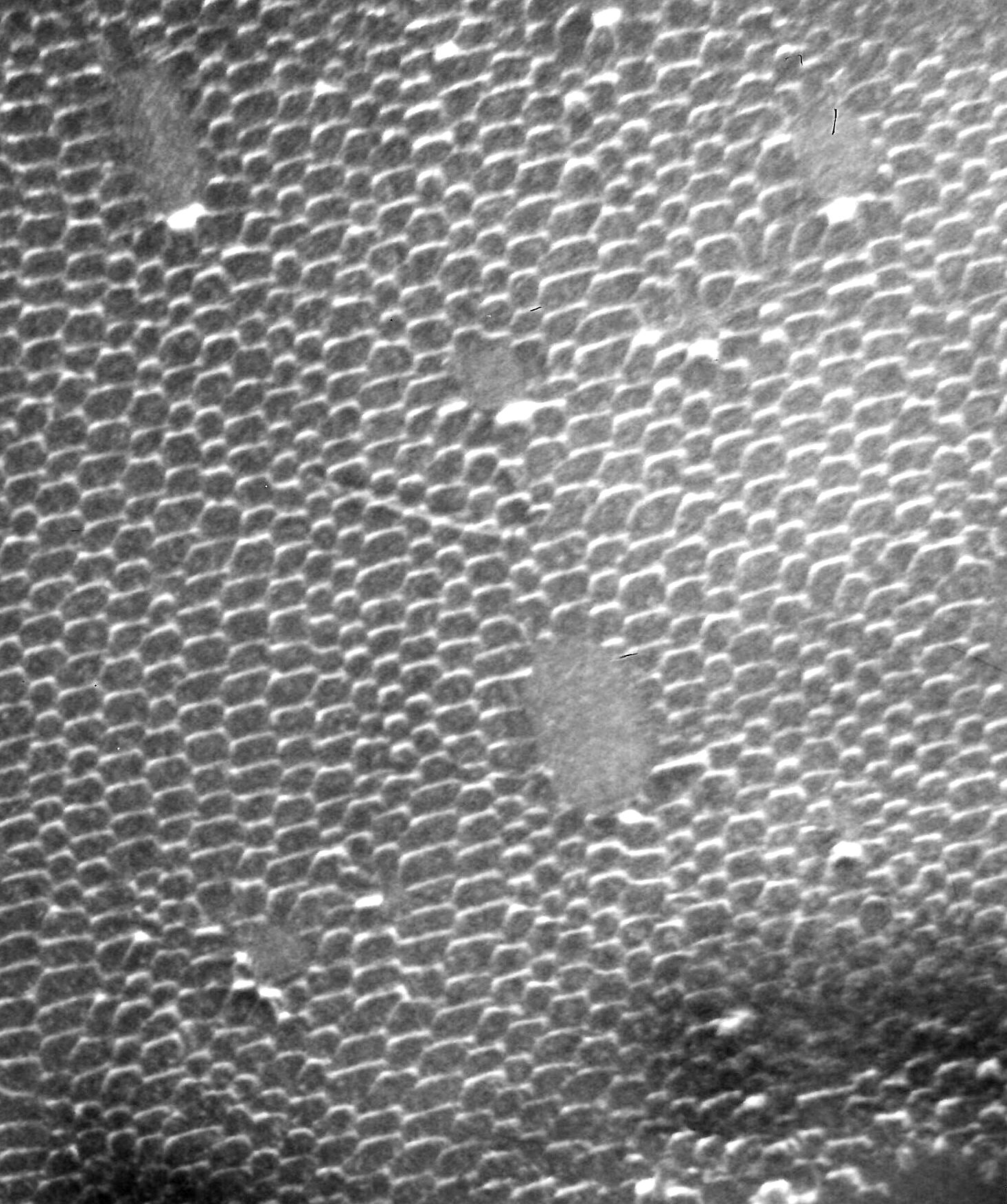
| | Similar to Fig. 7b). |
|
| |
|
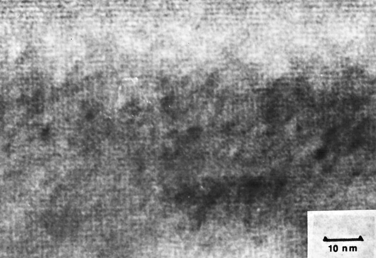
Fig. 8 in paper
Even the Philosophical Magazine, allowing rather large pictures and good print
quality, could not do justice to this picture.
Here you can see the networl, if just barely. |
| Image of a low-angle twist boundary on a (100) plane with a twist angle of 8' taken under multi-beam conditions. |
|
| |
|
 With frame

 3.1 TEM Work at Cornell University; 3.1 TEM Investigations of Grain Boundaries in Silicon
 Pictures to: 3.1 TEM Work at Cornell University; 3.1.1. TEM Investigations of Grain Boundaries in Silicon
 Pictures to: 3.1 TEM Work at Cornell University; 3.1.1. TEM Investigations of Grain Boundaries in Silicon
© H. Föll (Archive H. Föll)
![]() 3.1 TEM Work at Cornell University; 3.1 TEM Investigations of Grain Boundaries in Silicon
3.1 TEM Work at Cornell University; 3.1 TEM Investigations of Grain Boundaries in Silicon