|
Additional Pictures to: Process Induced Defects in Si Chips
|
| |
Part 1 Pictures in the Report and Publication |
| | Links to |
 |
In what follows you find
- High quality pictures of the ones shown in the Report or the publication.
- Additional pictures complementing those from above
- Some pictures not relating directly to 1.
|
|
 |
I will not provide much text for pictures that are contained in the report and/or
publication. Look it up there. |
 |
I start with some pictures showing the key to these investigations:
specimens being transparent to a HVTEM electron beam in huge areas – all the areas inside the specimen holder, in
fact. |
| | |
|
| |
 |
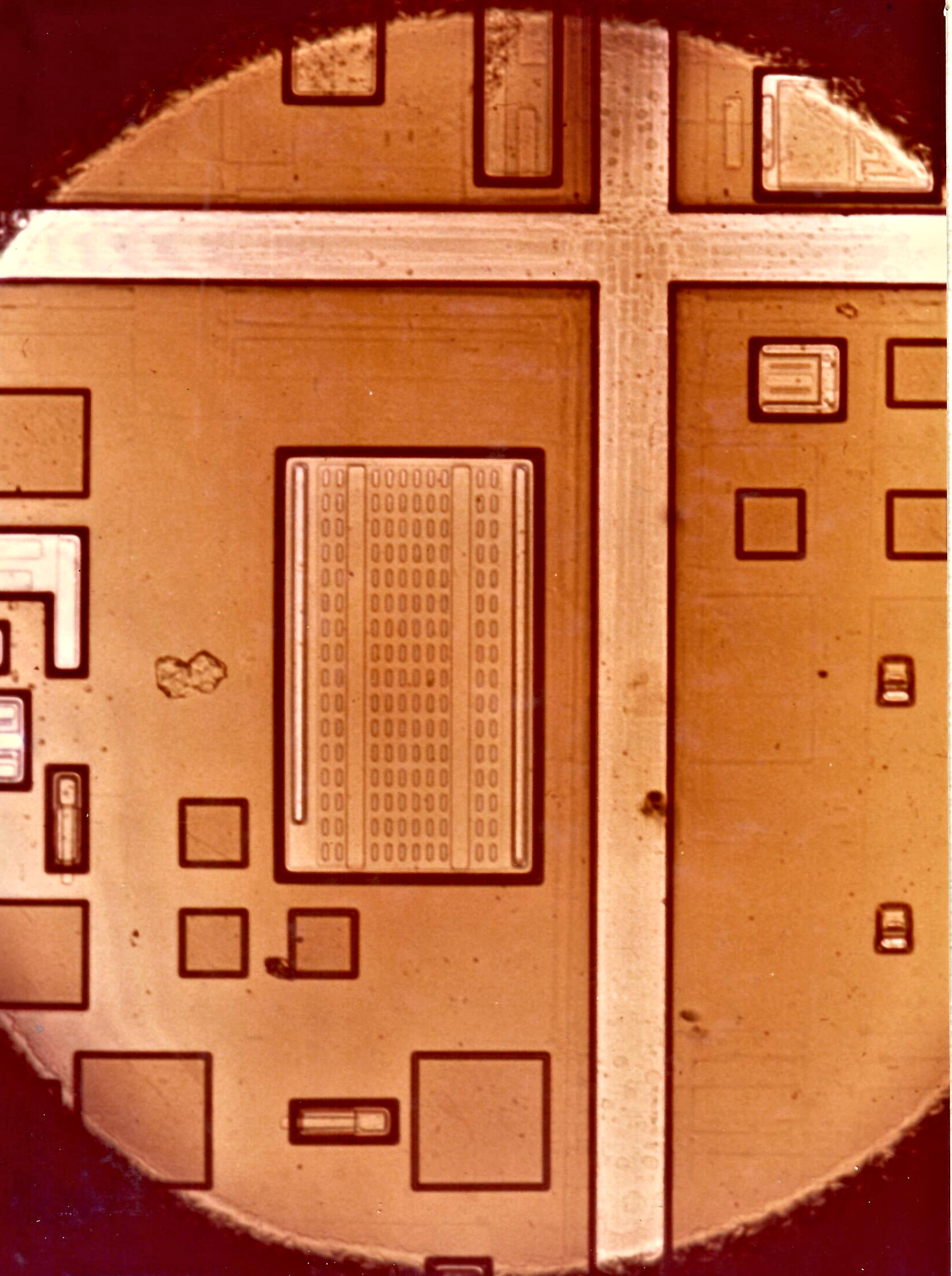
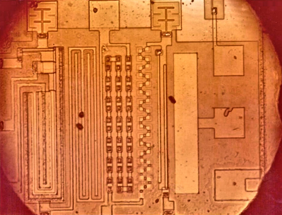
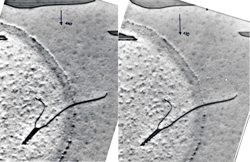
Looking through the mounted specimen in an optical microscope.
The diameter is 2.3 mm. We see
structurs belonging to an integrated circuit (IC) |
|
| |

| | Same as above but different IC. |
|
| |

|
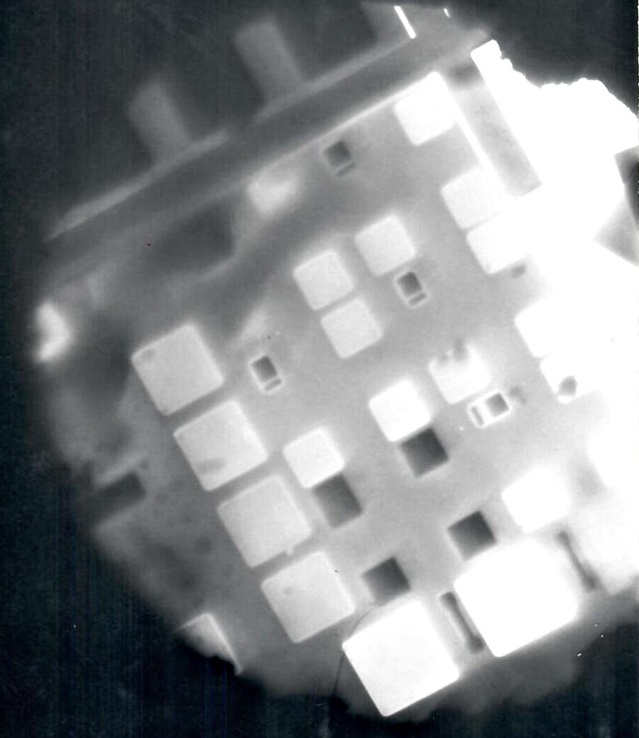
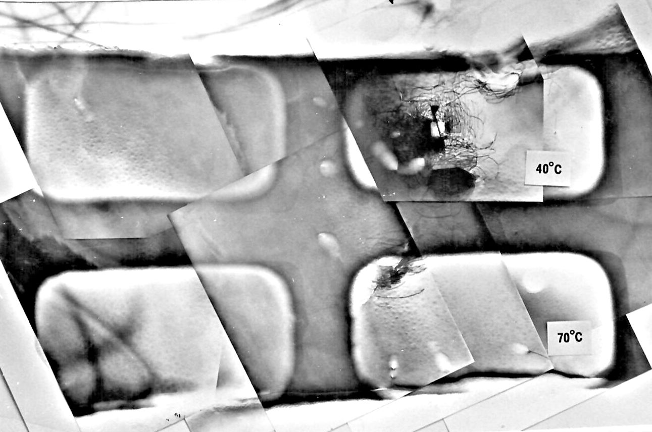
HVTEM picture of the whole specimen at a magnifications of 63 x!.
A very unusual picture at
a normally impossibly small magnification. |
|
| |
|
 |
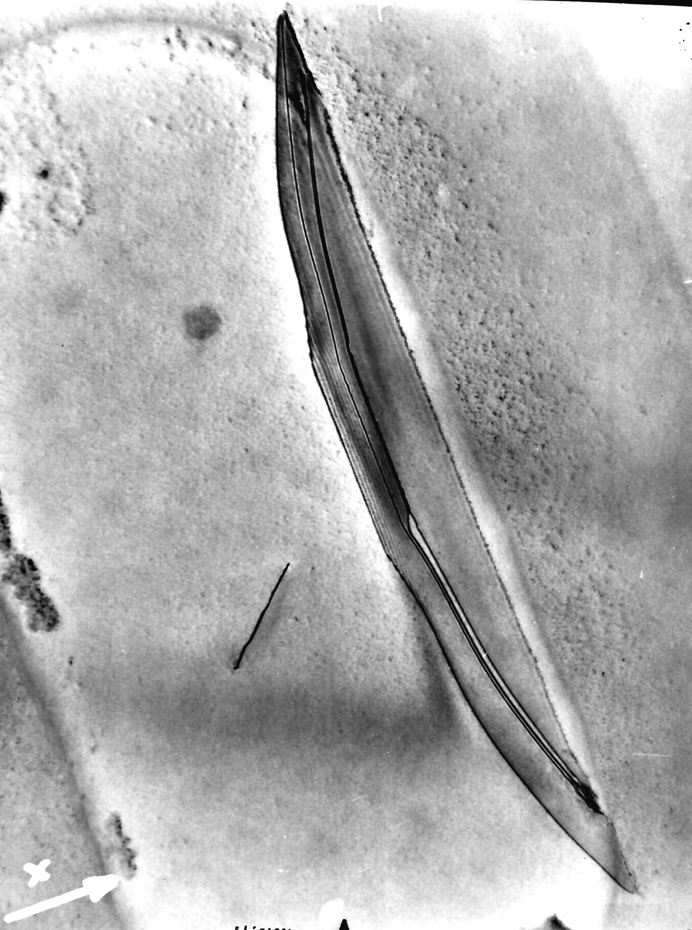
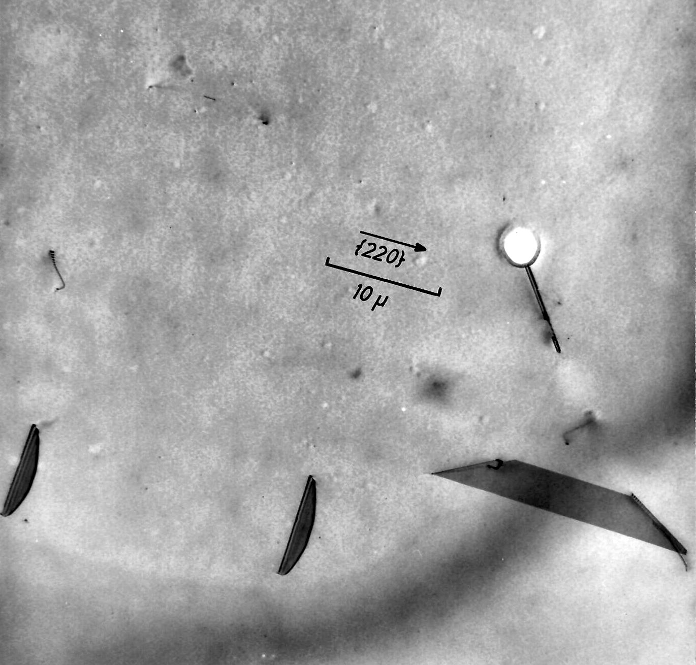
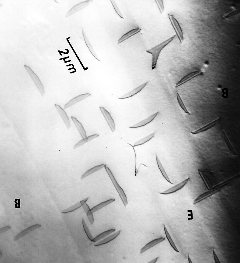
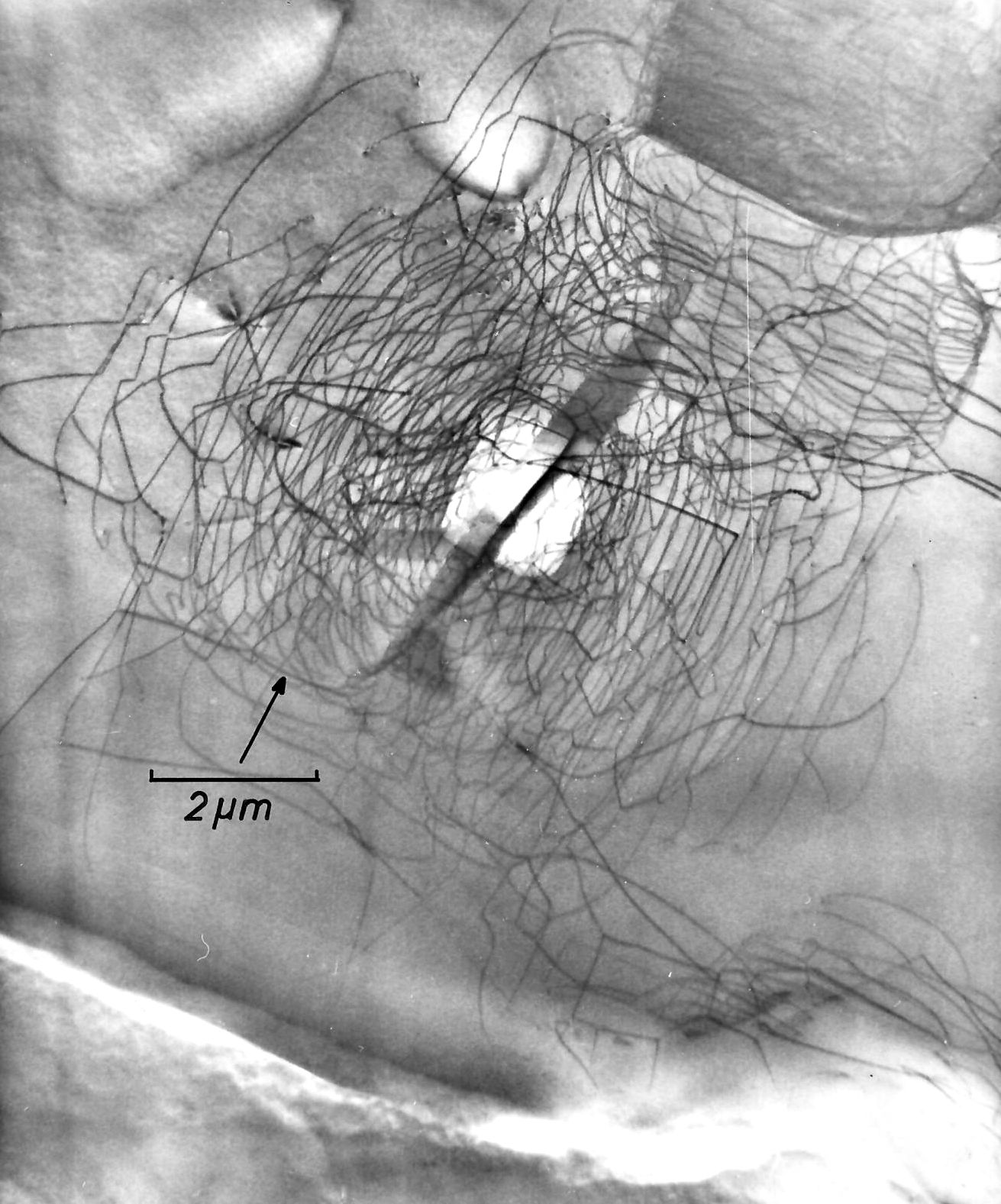
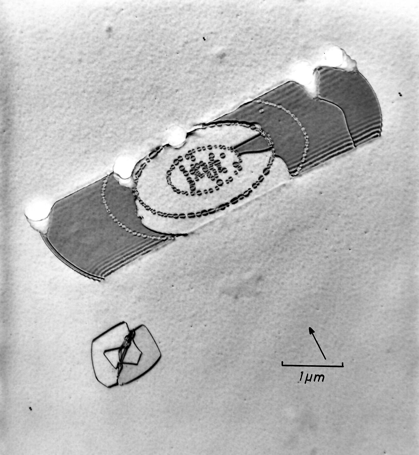
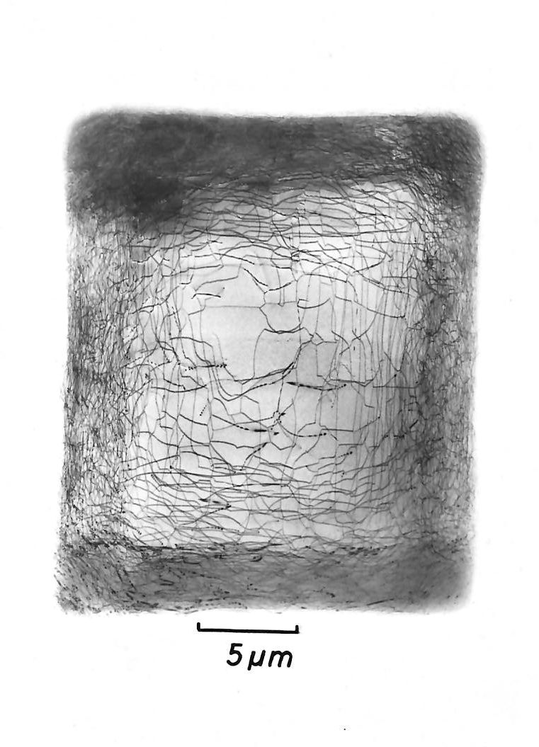
Next I show some of the HVTEM pictures used in the report. This does not include
all the TEM pictures because I didn't take all of them.
Some of these pictures were also used in the publications as
given in the caption. |
|
 |
I'm not offering explanations here. Refer to the report (or the publications
where appropriate) to learn about the meaning of these pictures |
 |
Now I need to to make a point. All these pictures may appear rather
common today (Oct. 2022). However, when we took them in 1975/76, they were spectacular.
Many of the defect structures
found have never seen before. In some cases we simply did not know what we witnessed. It took involved contrast analysis
and some cunning to figure out what has happened. It is hard today to imagine the excitement one experienced seeing some
of these things for the first time. |
| |
| |
| |

| | Fig. 13 in report. |
|
| |

| | Fig. 14a) in report.. |
|
| |

|
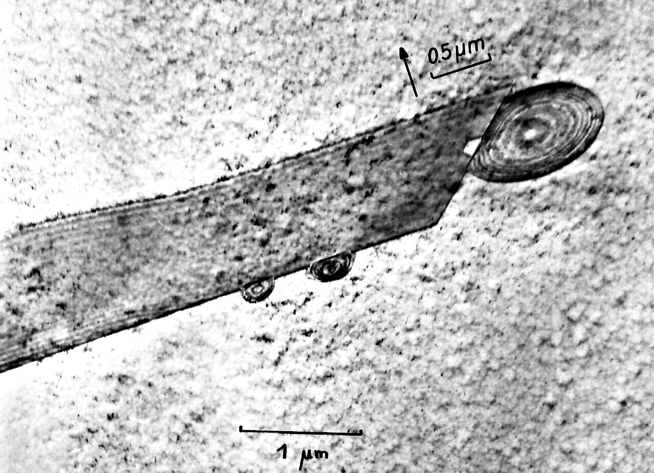
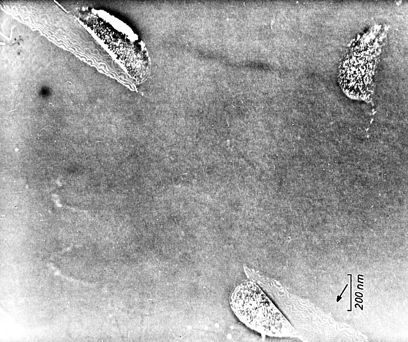
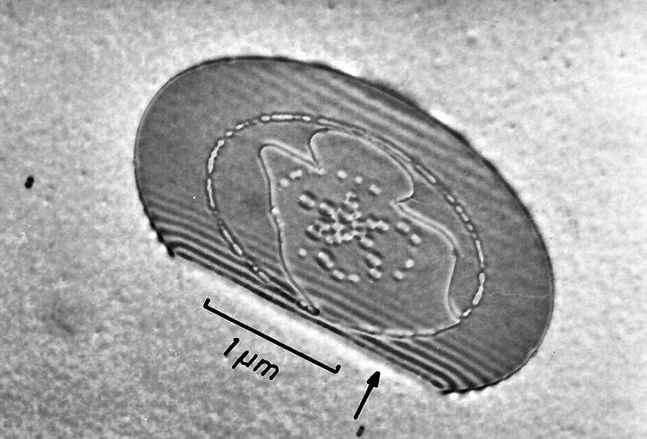
Fig. 14 b in report; Fig. 3b in publication..
Fig.3 (a) Stacking fault network, (b) nine-fold
stacking fault. |
|
| |

|
 |
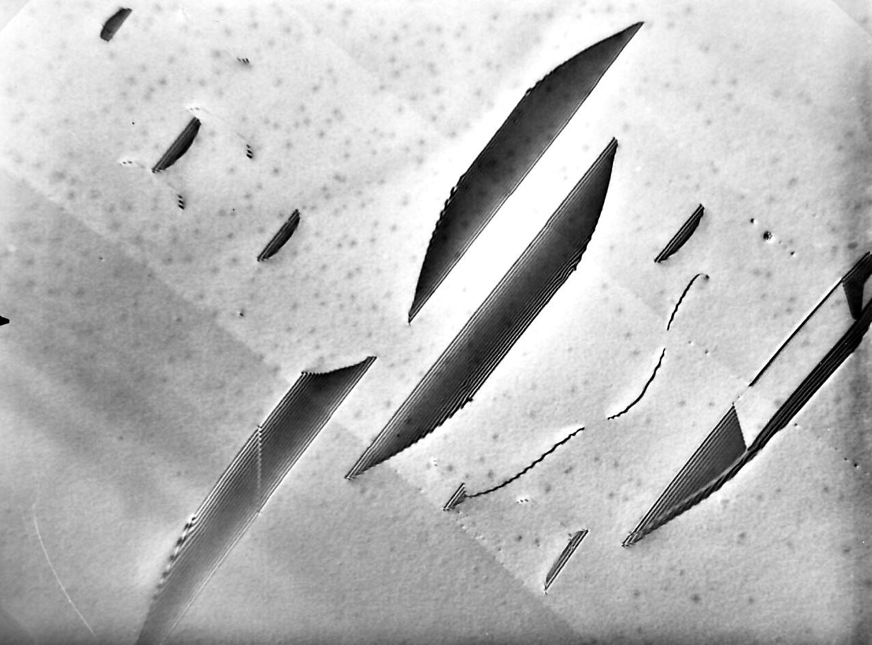
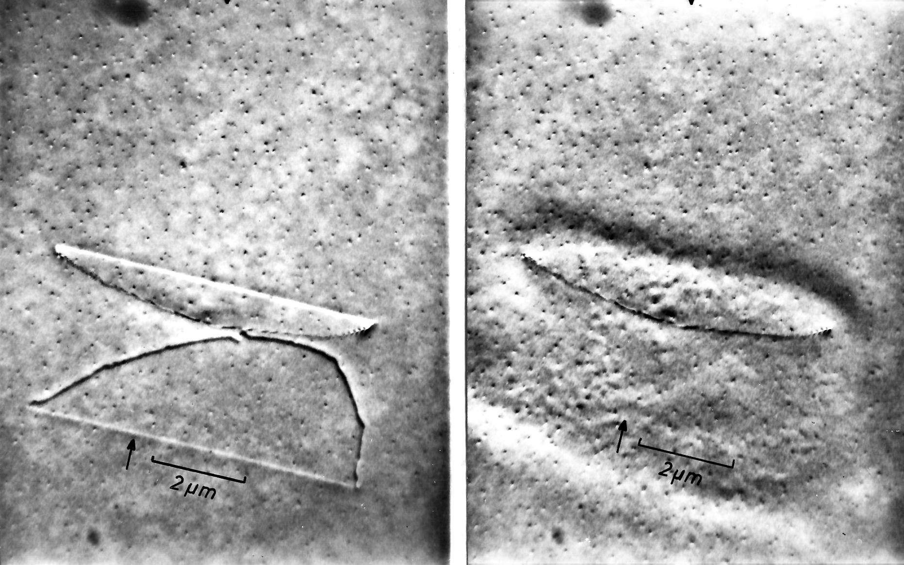
Auxiliary picture.
Multiple stacking fault from above out of contrast
plus another one
(in contrast) at the side. |
|
| |
 |
 |
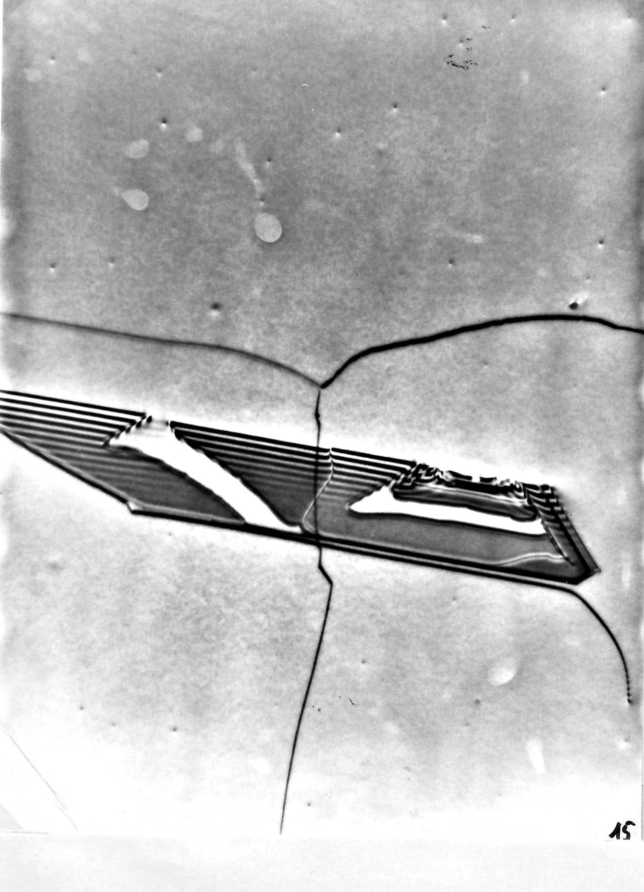
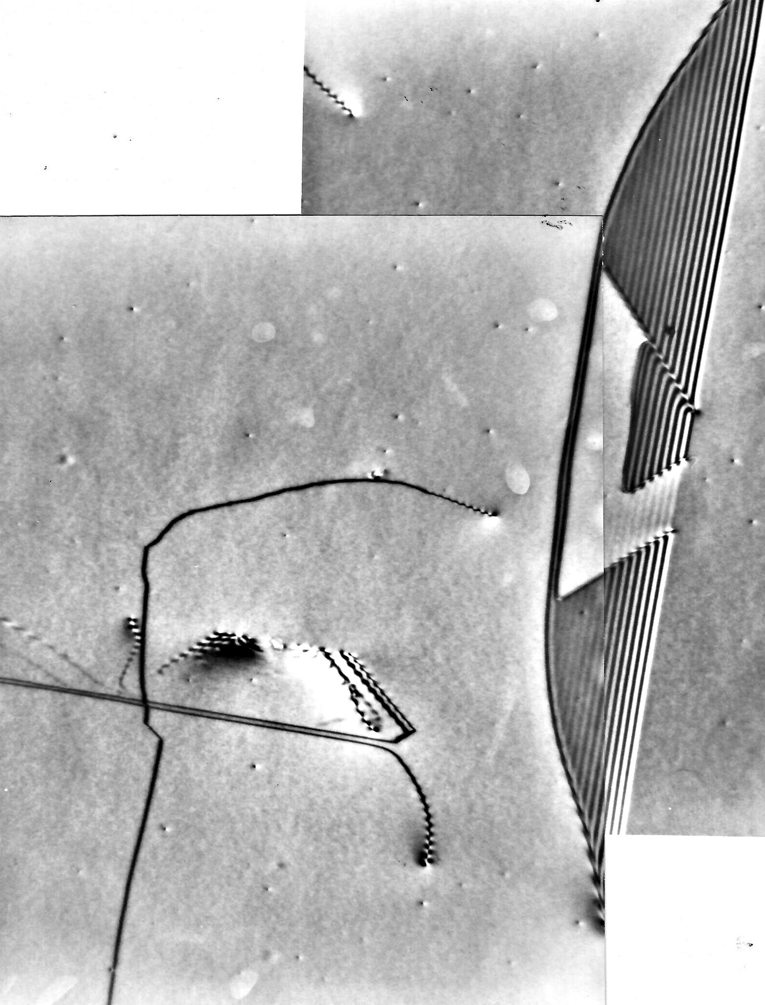
| Fig. 15 a) and b) in report. . |
|
| |
 |
| Detail to Fig. 18 in report. |
|
| |
 |
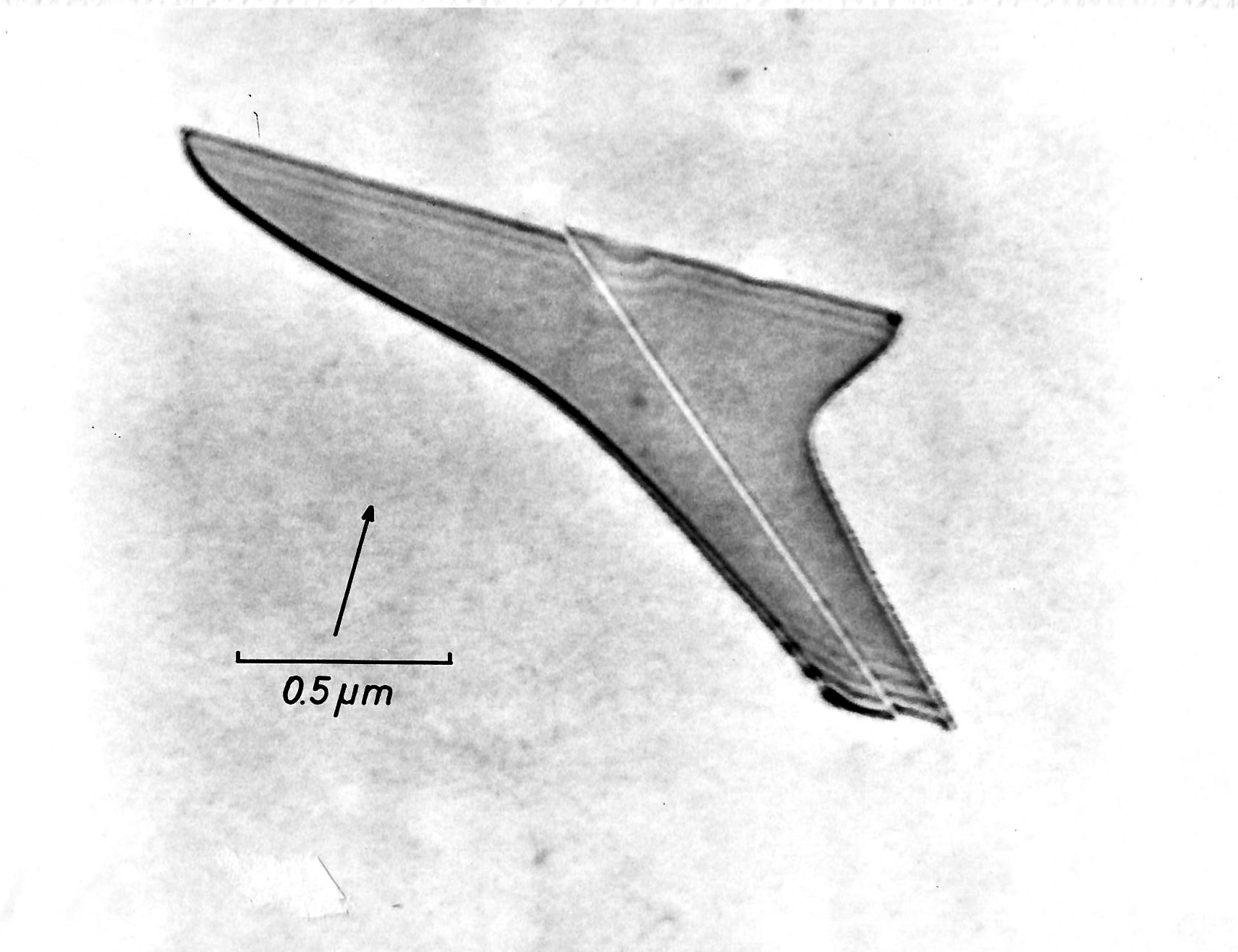
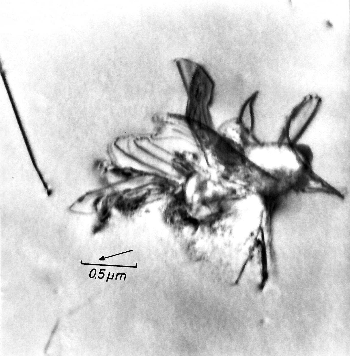
Fig. 19a) in report; Fig. 6 in publication.
Fig.6 Typical example of an unfaulted sailing boat
SF. |
|
| |
 |
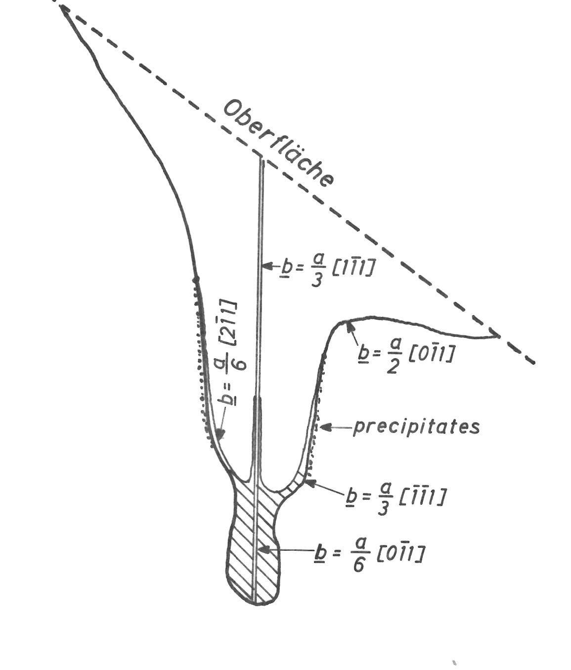
. Fig. 19b) in report; Fig. 7a) in publication
Fig.7 (a) Sailing boat stacking fault after an
unfaulting rcaction. (b) Schematical drawing of its crystallographic structure. (below) |
|
| |
 |
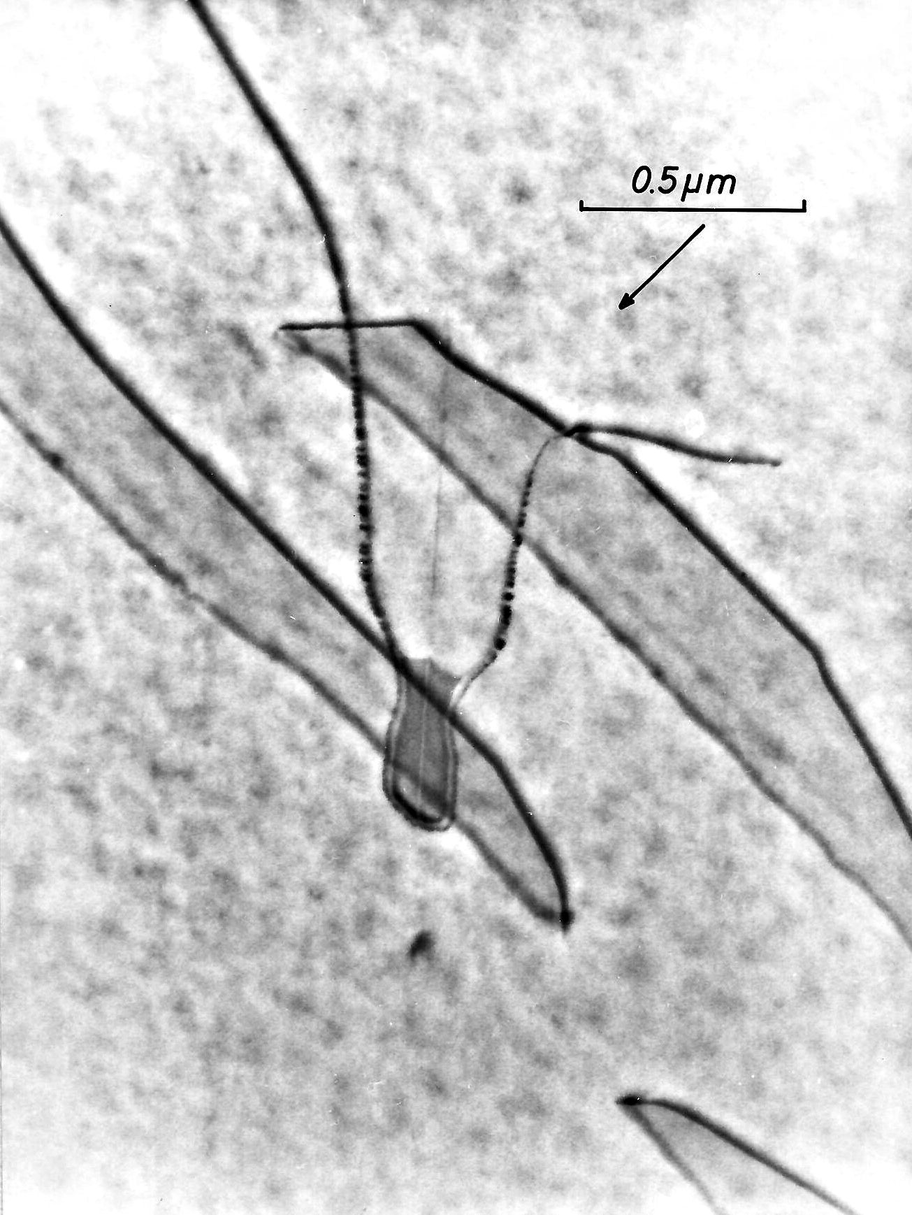
Fig. 19c) in report; Fig. 7b) in publication.
This fellow combines all possible kinds of dislocations
in Si plus a stacking fault.
The unfaulting reactions is rarely seen "in-situ". |
|
| |
|
 |
What follows are a few auxiliary pictures showing this remarcable stacking fault complex |
| | |
| |

|
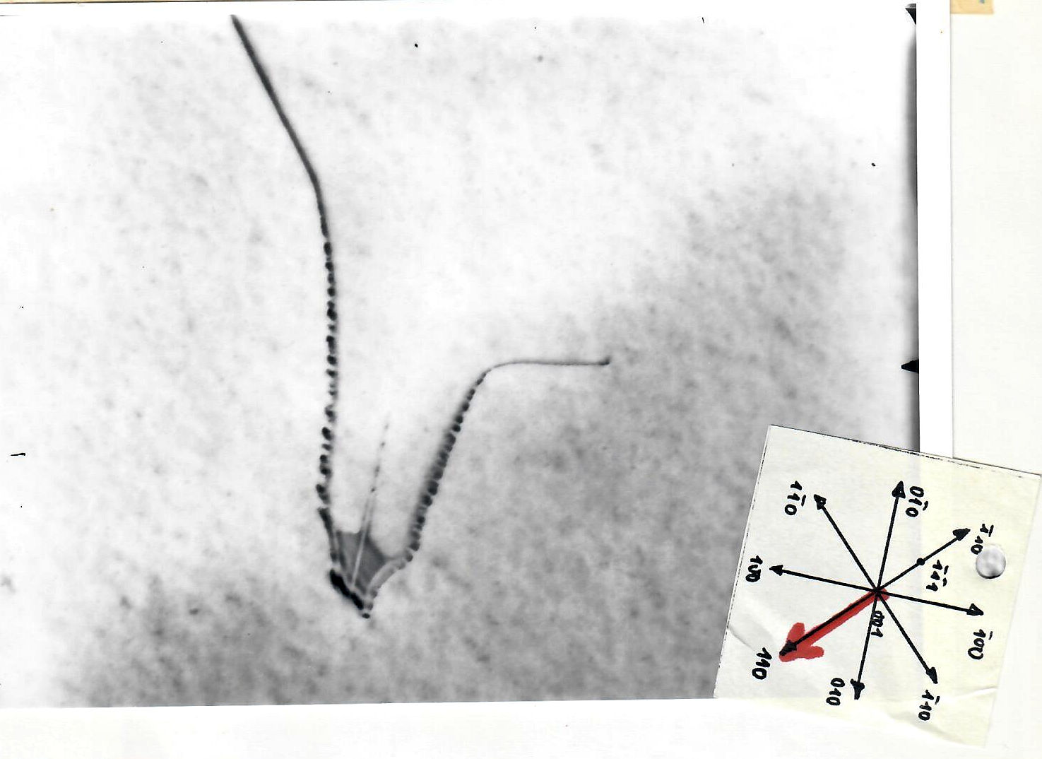
Relating to Fig. 19c) in report; Fig. 7b) in publication.
One of the many stereo sets taken |
|
| |
 |
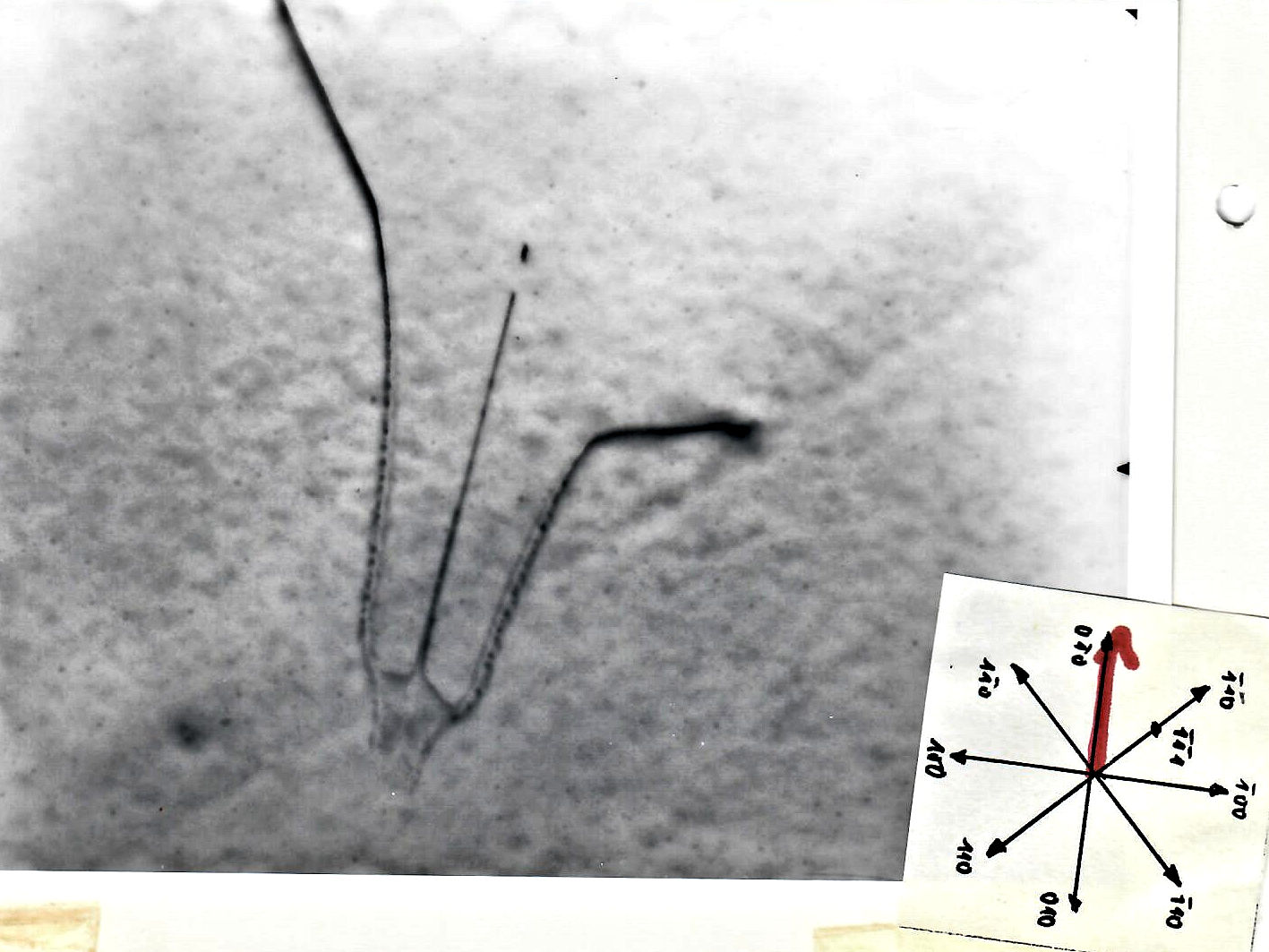
Relatuing to Fig. 19c) in report; Fig. 7b) in publication.
This and the following pictures
allow contrast analysis. |
|
| |
 |
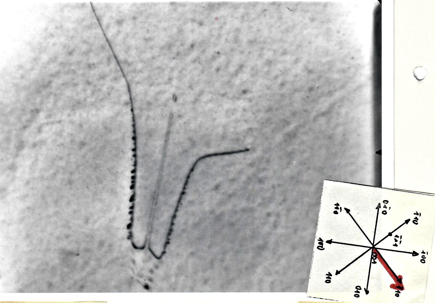
Relatuing to Fig. 19c) in report; Fig. 7b) in publication.
This picture allow contrast analysis. |
|
| |
 |
Relatuing to Fig. 19c) in report; Fig. 7b) in publication.
This picture allow contrast analysis. |
|
| |
 |
| Fig. 50 in report. |
|
| |

| | Enlarged part of Fig. 50 in report; Fig. 2b in publication. |
|
| |

| | Fig. 55 in report, Fig. 10a) in publication. |
|
| |
|
 |
Here are a few pictures only used in the publication: |
| | |
|
| |

| | Fig. 1a in publication. |
|
| |

| | Fig. 2A in publication. |
|
| |

| | Fig. 3 in publication. |
|
| |

| | Fig. 8 inb publication. |
|
| |

| | .Fig. 9a) in publication |
|
| |

| | Contains Fig. 9b) in publication |
|
| |

| | Fig. 10b in publication. | | |
| Links to |
|
 With frame

 2.4 Process Induced Defects in Si Chips (Investigated in a HVTEM)
 Kristallfehler in hochintegrierten Schaltkreisen aus Silizium
 Additional Pictures to: Process Induced Defects in Si Chips
 Additional Pictures to: Process Induced Defects in Si Chips
© H. Föll (Archive H. Föll)
