Additional Pictures to: Process Induced Defects in Si Chips


Part 2   Auxiliary Pictures 1

  Links to
In what follows you find some auxiliary pictures illustrating some point.
I could illustrate one major point but, out of the goodness of my heart, will not do so. The point is:
For any picture contained in the publication / reports, thee are at least 50 or more taken but not shown- And for any picture taken, there are many observations where some feature (“stacking fault in emitter of transistor 57 in sample 19”). In other words: a lot of time was spent at the microscope (and later in the dark room developing negatives and printing pictur es)
     
 
Defects in integrated circuits
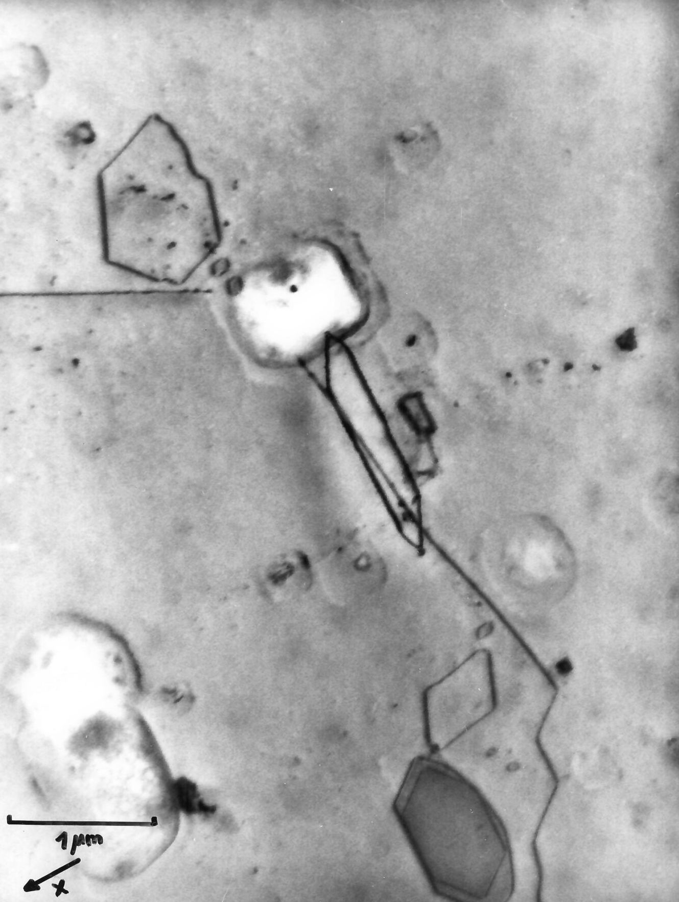
Auxiliary picture. Similar to Fig. 13 in report..
 
Defects in integrated circuits
Auxiliary picture. Same sample as Fig. 13 in report.
 
Defects in integrated circuits
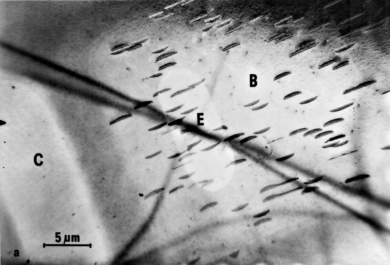
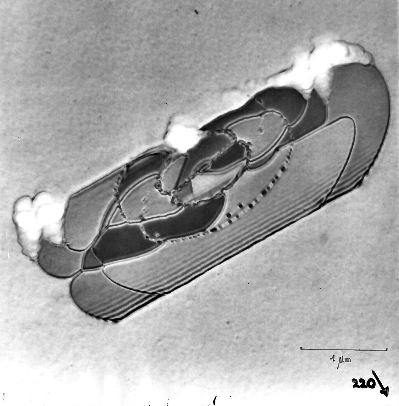
Auxiliary picture. Similar to Fig. 18 in the report and Fig. 5 in the publication.
Small stacking faults only in the emitter region, Only on of two types is visible
 
Defects in integrated circuits
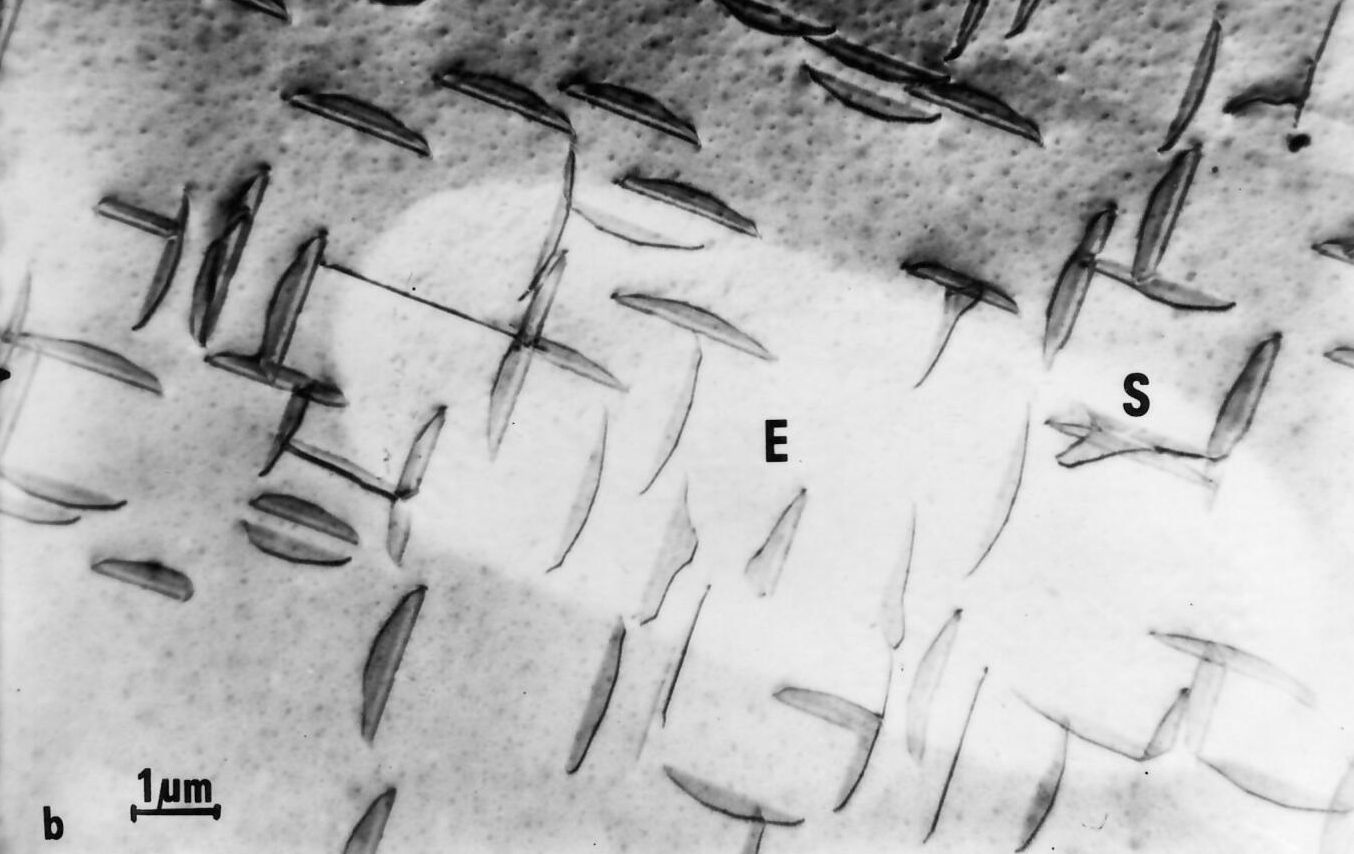
Auxiliary picture. Similar to Fig. 18 in the report and Fig. 5 publication; as above.
Small stacking faults only in the emitter region, Both types are visible, including a "sailing boat" stacking fault
 
Defects in integrated circuits
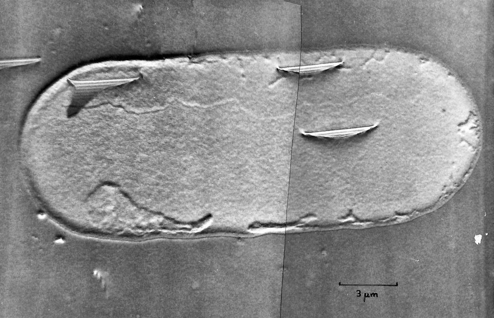
Auxiliary picture. Similar to Fig. 18 in the report and Fig. 5 publication; as above.
There is a deadly "sailing boat" stacking fault in the emitter
 
Defects in integrated circuits
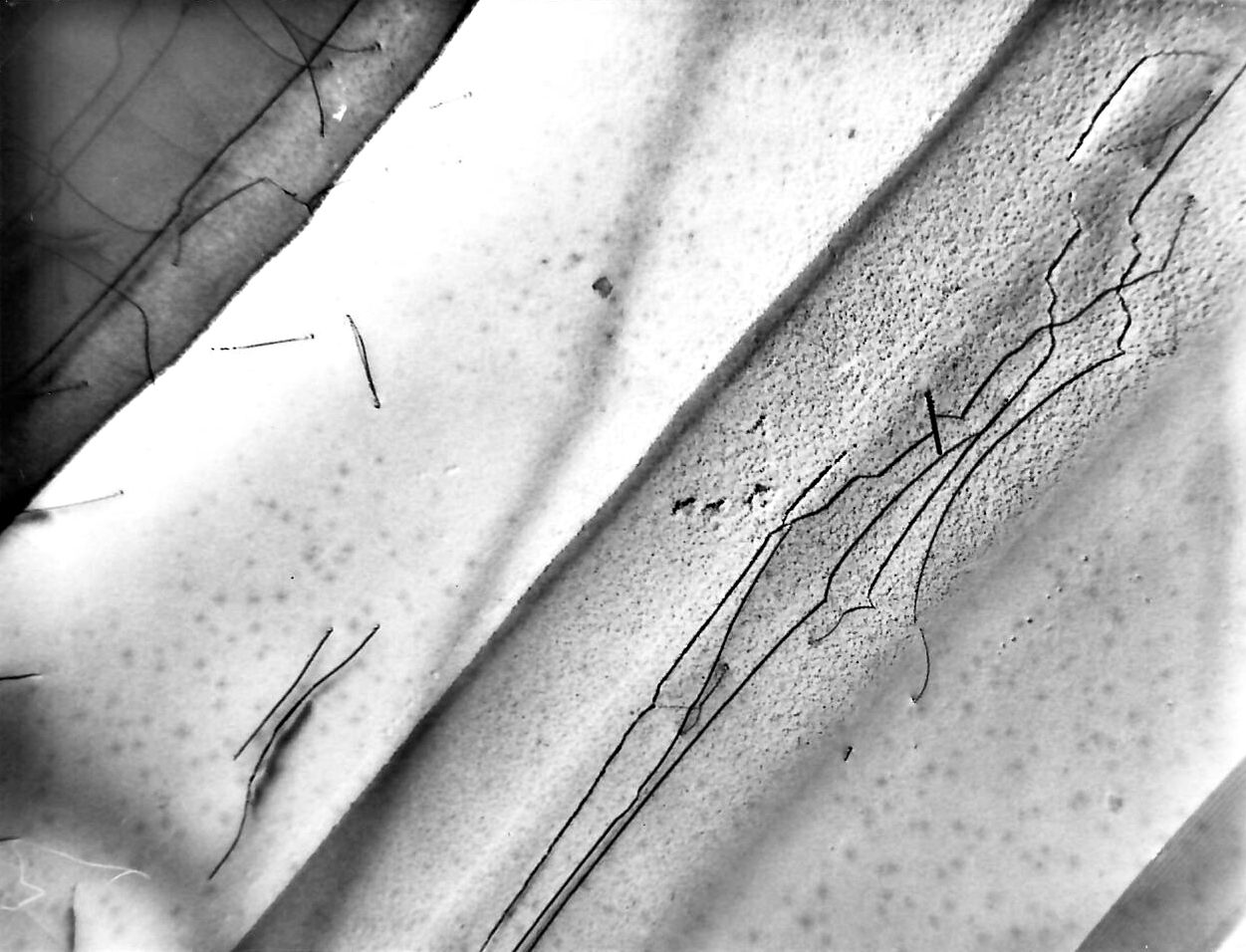
Auxiliary picture. Similar to Fig. 54 in Report..
 
Defects in integrated circuits
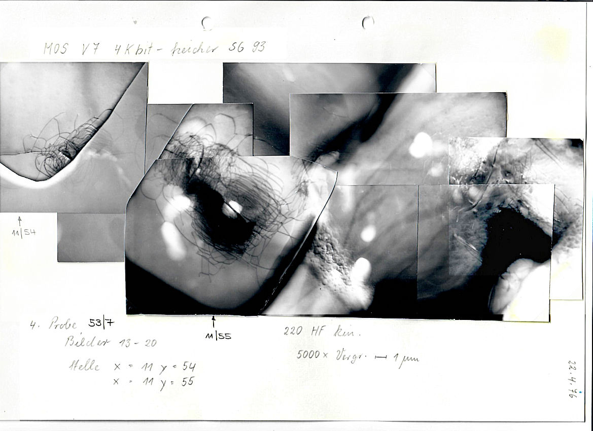
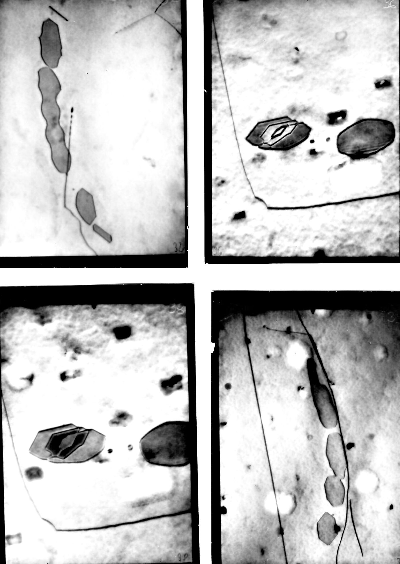
Auxiliary picture .Relates to Fig. 50 uin the report and Fig. 2a) in the publication.
This is a page from our documentation records. It also illustrates the problems with the very high contrast due to thickness variations and how much work was necessary in the dark room to come up with a composite like this.
 
Defects in integrated circuits
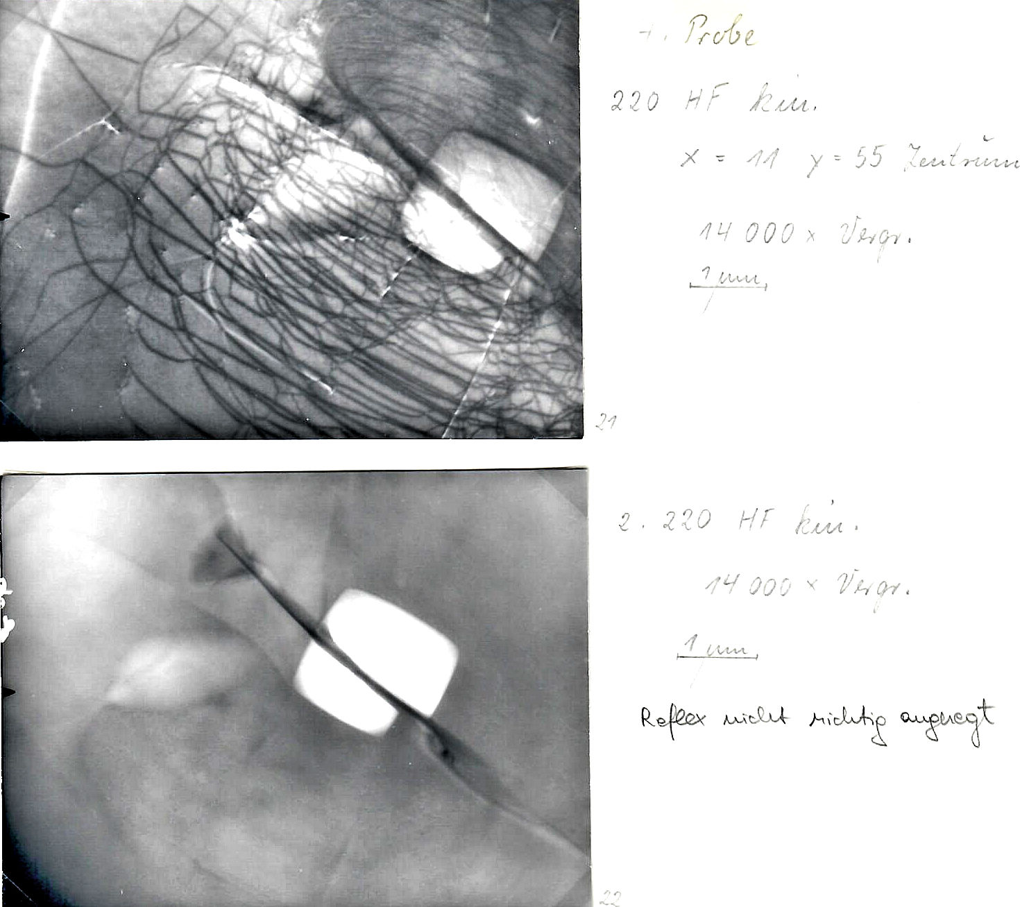
Auxiliary picture. Details to t e picture above.
 
Defects in integrated circuits
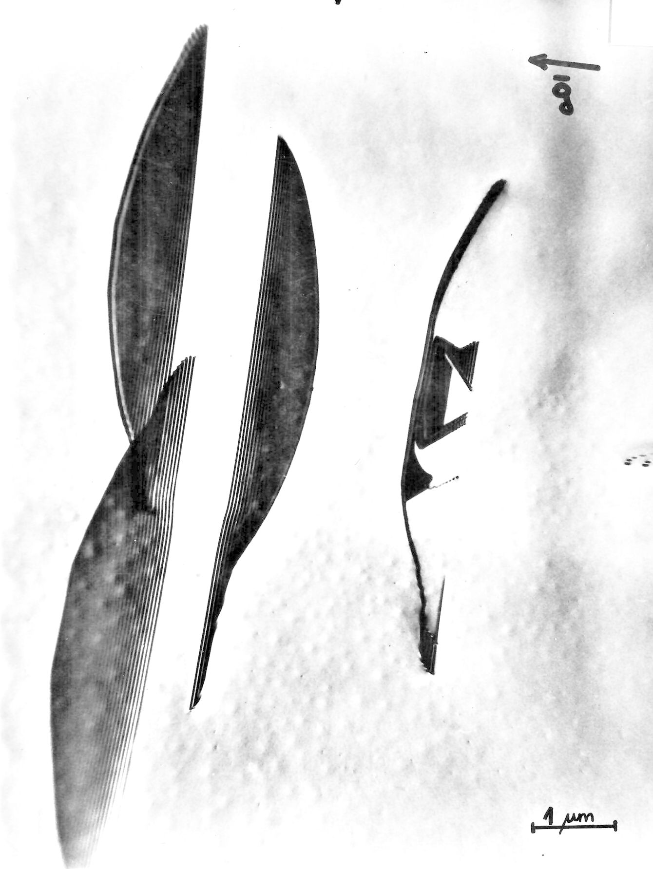
Auxiliary picture.
Illustrating what an excess of point defects (I.e. interstitials from oxidation) plus stress can do if there is some nucleation..
 
Defects in integrated circuits
Auxiliary picture. .
Same as above
 
Defects in integrated circuits
Auxiliary picture. .
Same as above. Page from our "scrap book"
   
 
Defects in integrated circuits
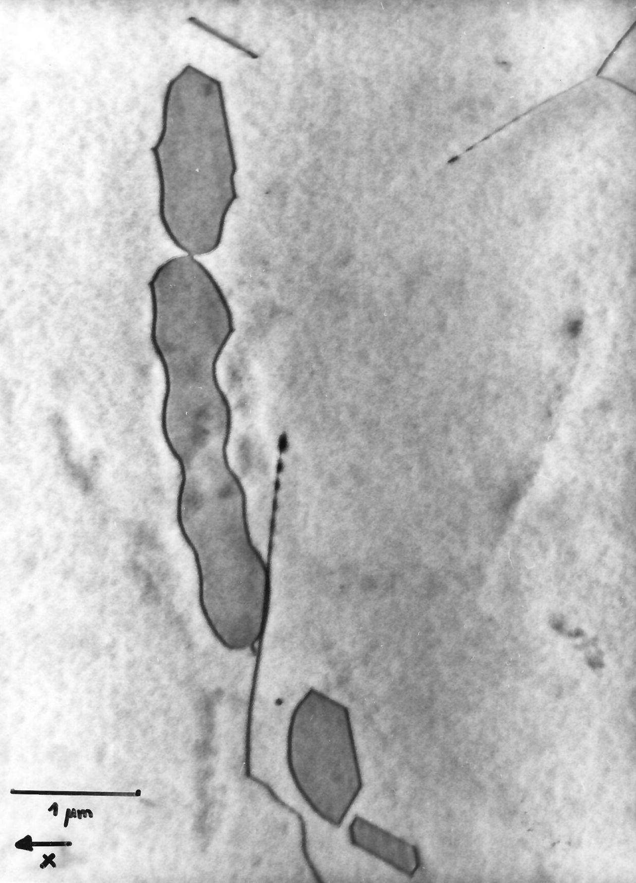
Auxiliary picture. .
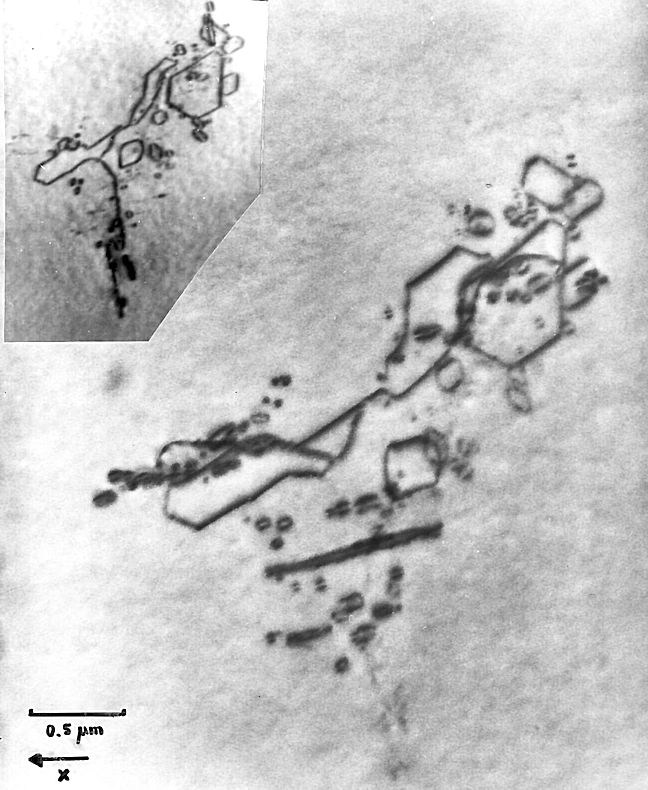
Same as above. Probably metal precipitates.
Illustrating that ultimately nucleation controls almost verything and that
the nuclei are often if not always small metal precip itates.
The inset shows the cluster under differnt diffraction conditions.
   
  Links to
   

With frame With frame as PDF

go to Additional Pictures to: Process Induced Defects in Si Chips

go to Additional Pictures to: Process Induced Defects in Si Chips

© H. Föll (Archive H. Föll)