Additional Pictures to: Process Induced Defects in Si Chips


Part 2   Auxiliary Pictures 2

  Links to
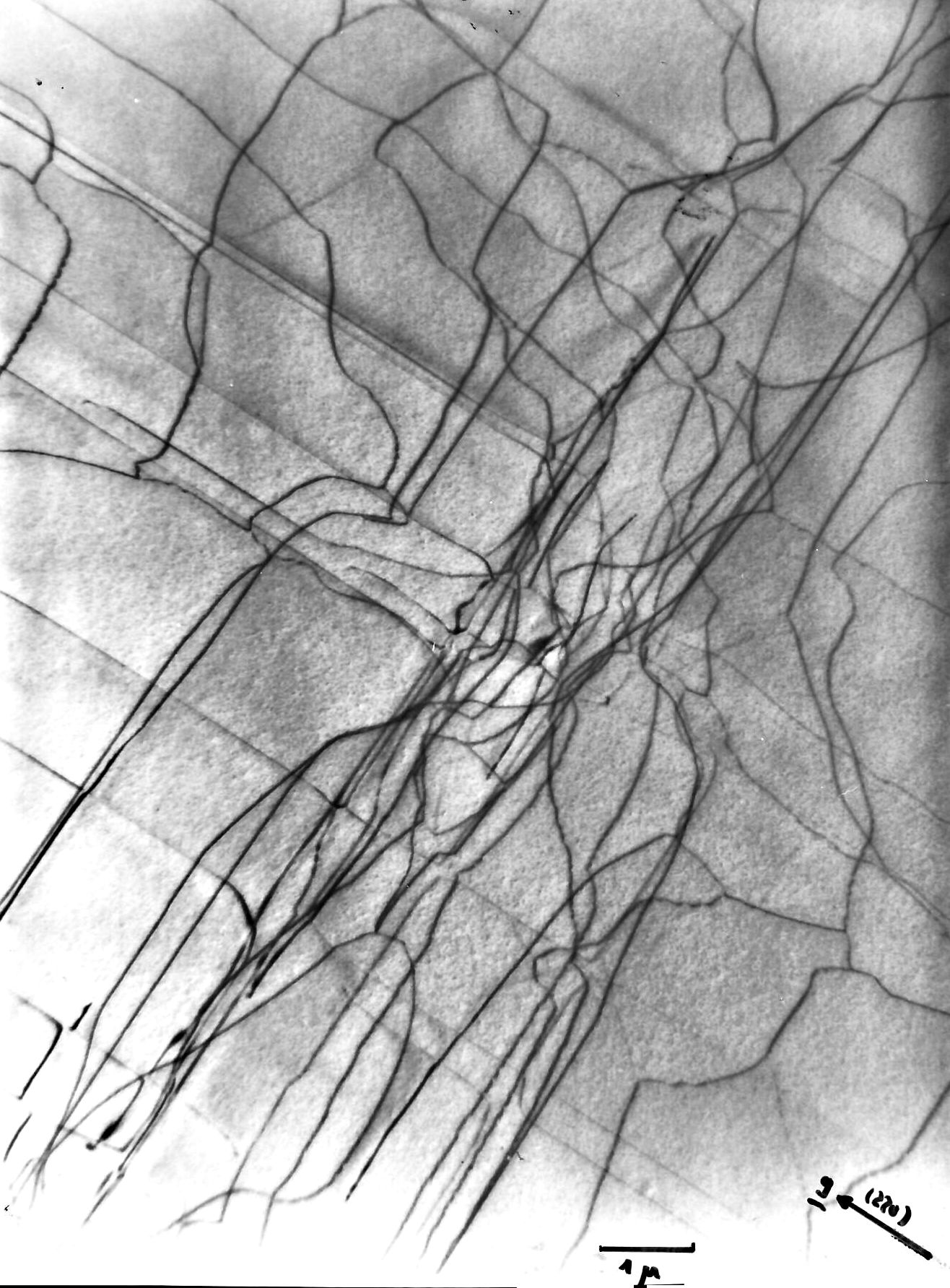
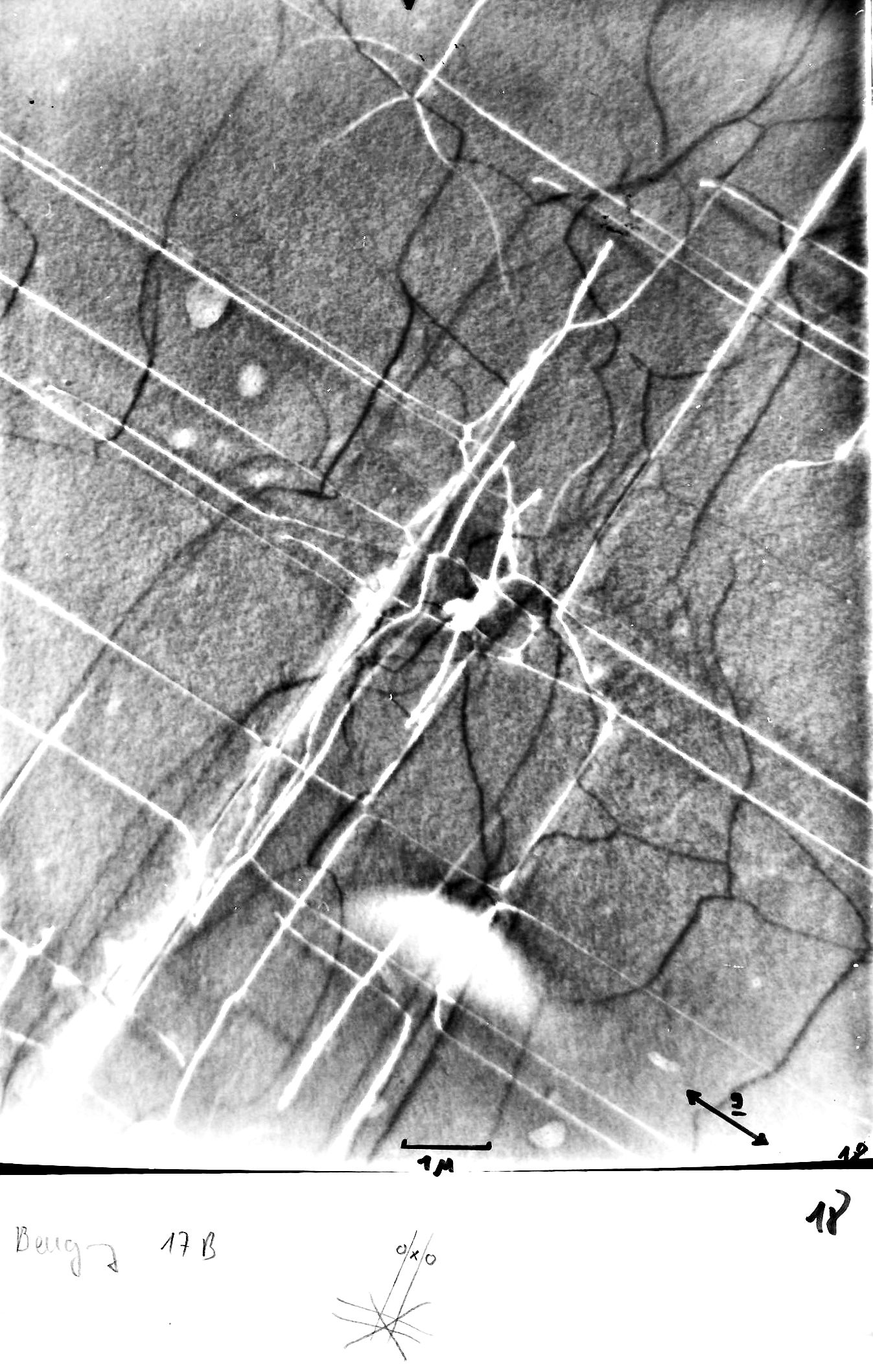
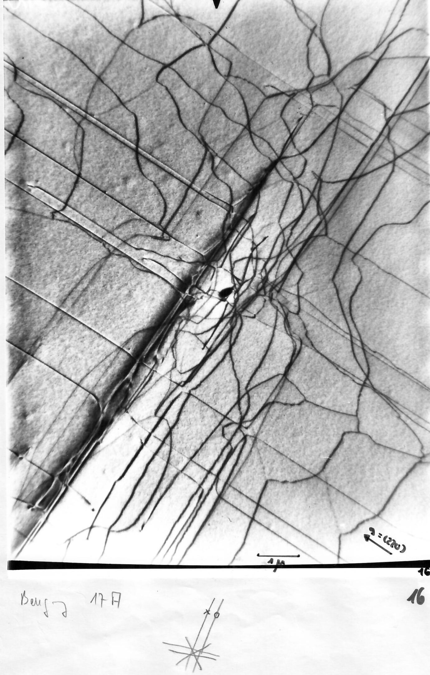
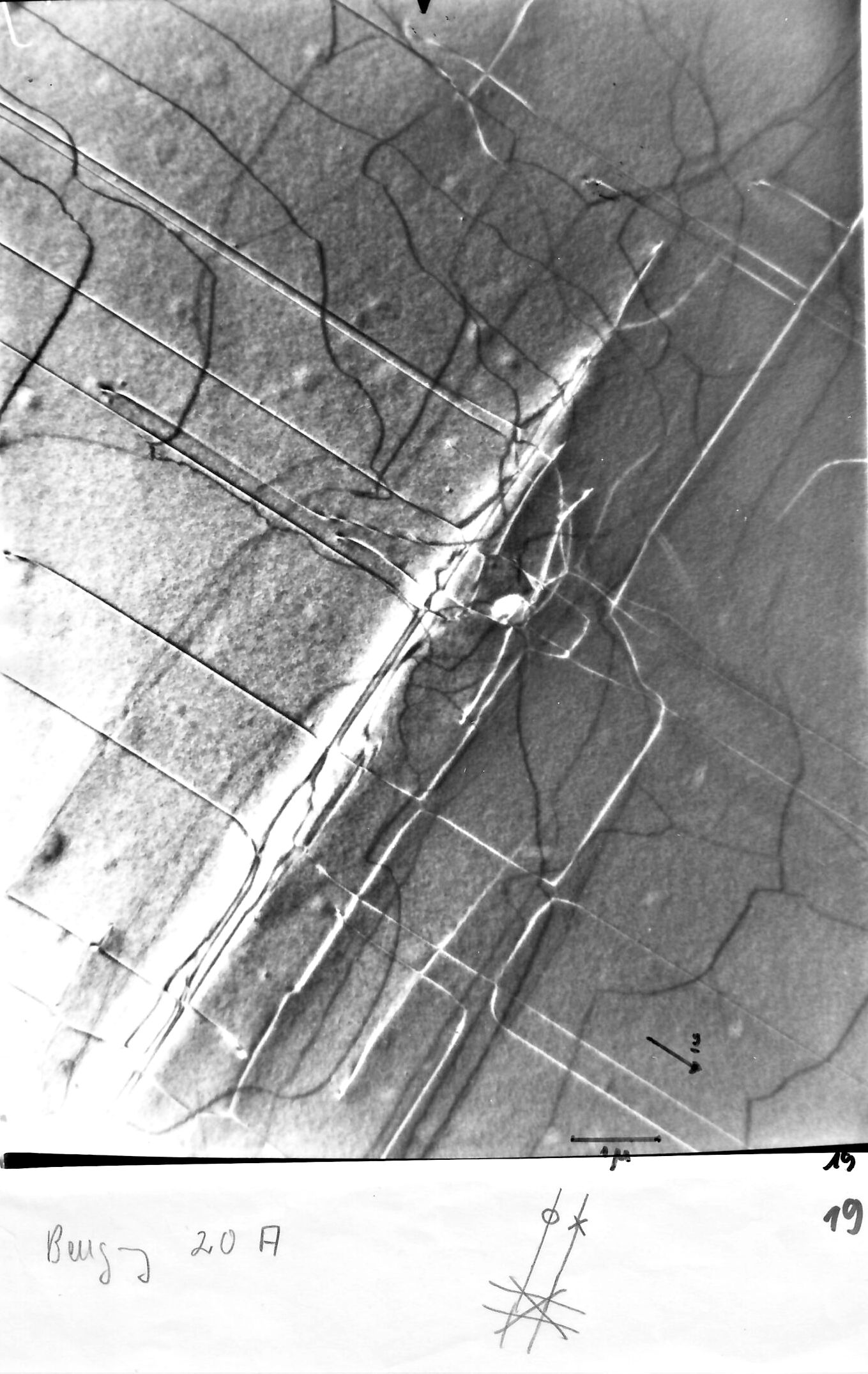
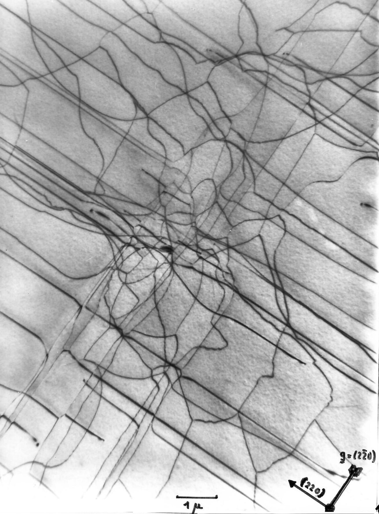
In what follows you find a collection of defects that look like stacking faults on a first glance. However, their contrast behavior is often not quite what one would expect and it turned out that we had complex structures involving micro twins and various dislocations.
Once more I want to emphasize that we had had the privilege to see these peculiar Si defects for the first time. Nobody, we sincerely believe, had seen anything like that before
     
 
Defects in integrated circuits
Auxiliary picture. Similar to Fig. 13 in report..
Note that little etch pits denote dislocations ending at the surface.
Note also that one etch pit denotes an "invisible" dislocation while there is no etch pit at
the line denoting strong contrast change. Microtwins are involved here
(and in some of the following pictures)
 
Defects in integrated circuits
Auxiliary picture. Similar to Fig. 13 in report.
Not etch pits or the lack thereof.
 
Defects in integrated circuits
Auxiliary picture. Similar to Fig. 13 in report
 
Defects in integrated circuits
Auxiliary picture. Similar to Fig. 13 in report
 
Defects in integrated circuits
Auxiliary picture. Similar to Fig. 13 in report
 
Defects in integrated circuitsTD>
. Auxiliary picture. Similar to Fig. 13 in report
Page from our protocols, showing one of the many stereo pairs we took and some
contrast analysis by changing diffraction vectors
 
Defects in integrated circuits
Auxiliary picture. Similar to Fig. 13 in report
Page from our protocols, showing one of the many stereo pairs we took and some
contrast analysis by changing diffraction vectors.
 
Defects in integrated circuits
Auxiliary picture. Similar or Fig. 1 in publications.
A (huge for today standards) bipolar transistor full of dislocations
 
Defects in integrated circuits
Auxiliary picture. As above.
Here you see a diffraction pattern and you also see why it is almost useless to print them.
The contrast is typically far too large to be reproduced on photo paper.
There is also a low-mag picture of the whole transistor.
 
Defects in integrated circuits
Auxiliary picture.
As above.
 
Defects in integrated circuits
Auxiliary picture.
Same as above. We also see an extremely low-mag
picture of the whole sample (shown before)
The perfectly white areas consist of Si much thinner than the rest.
Once more, you can't compress the contrast range present on the screen or on the negative to fit on photo paper.
 
Defects in integrated circuits
Auxiliary picture. Goes with most stacking fault parts in the report / publication; especially the "sailing boat" types
. (Multi) stacking fault. First nucleated (presumably) by a metal precipitate. The the Frank dislocations at its edges acted as nuclei for further metal precipitation
 
Defects in integrated circuits
Auxiliary picture.
Misfit dislocations produced by stress induced by heavy doping (by diffusion).
   
 
Defects in integrated circuits
Auxiliary picture; same as above
Different diffraction vector as indicated
   
 
Defects in integrated circuits
Auxiliary picture; same discolorations as above
We have a weird diffraction effect here, not reported in the literature then.
Imaging in a symmetric three-beam case (as indicated in the drawing) produced
oscillations of the dislocations contrast from black to white, obviously with depth.
Possibly only observable in very thickly samples in a HVTEM
 
Defects in integrated circuits
See caption below
 
Defects in integrated circuits
+g / -g pictures
Just changing the sign of the diffraction vector produced weird contrast phenomenae.
Some dislocations showed black-white contrast with a sign change of the black-white vector,
some changed from black to white, some stayed black… This demonstrates that we had all
kinds of problems then that one doesn’t have now. It was not always clear what we
encountered (that will happen if you see something for the first time) and contrast
theory wasn’t developed to a point where you always understood what your microscope was doing
  Links to

With frame With frame as PDF

go to Additional Pictures to: Process Induced Defects in Si Chips

go to Additional Pictures to: Process Induced Defects in Si Chips

© H. Föll (Archive H. Föll)