| |
Pictures to: 2.3 Swirl Defects in Si (Investigated in a HVTEM)
Part 1 |
 |
Bernd Kolbesen's and
my Investigation of swirl defects in Si caused some mild sensation among all the connoisseurs world-wide (at least around
50) and resulted in several publications. I therefore will not refer to the fig. numbers in all that printed matter but
discuss the following pictures shortly in the caption. |
|
 |
Once more, only a small fraction of all the pictures taken was published. Analyzing
the nature of a dislocations loop (vacancy or interstitial) from TEM images was (and is) a tricky job with lots of pitfalls
and we took loads of pictures with different diffraction conditions to be on the safe side. |
|
 |
The pictures are very distinct, you will find then easily in my thesis or in
the publications., That's why I don't give figure captions. |
| |
| |
| |
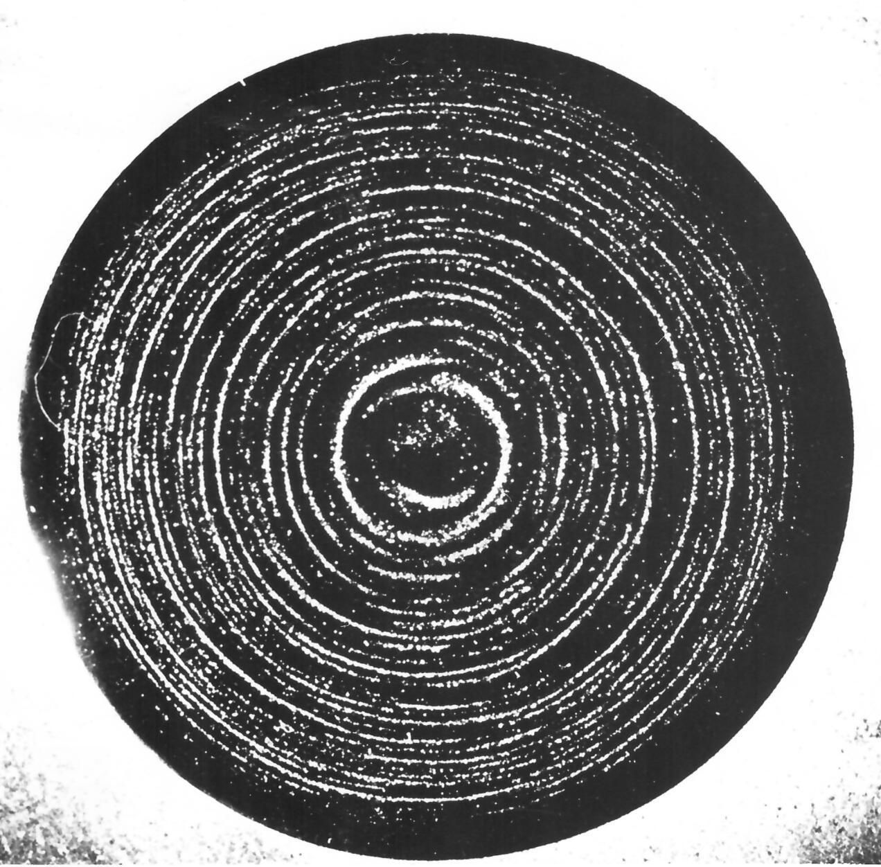 |
Etch pattern of swirl defects on a 33 mm float-zone (FZ) Si crystal.
It shows why the defects revealed are called "swirl defects".
This si a "famous" picture
shown may times. It is,. however "low resolution" - not showing
details of the etch pattern - and a bit atypical
because most "swirl patterns" weren't
quite that nicely spiralling from the outside to the center.- |
|
| |
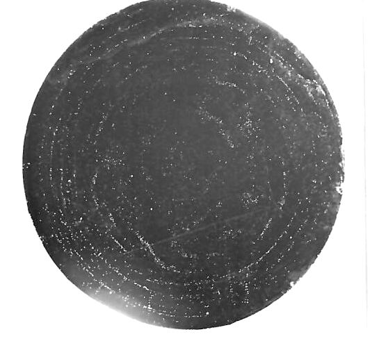 |
| Etch pattern of swirl defects on a 33 mm float-zone (FZ) Si crystal; somewhat less showy than the one above.. |
|
| |
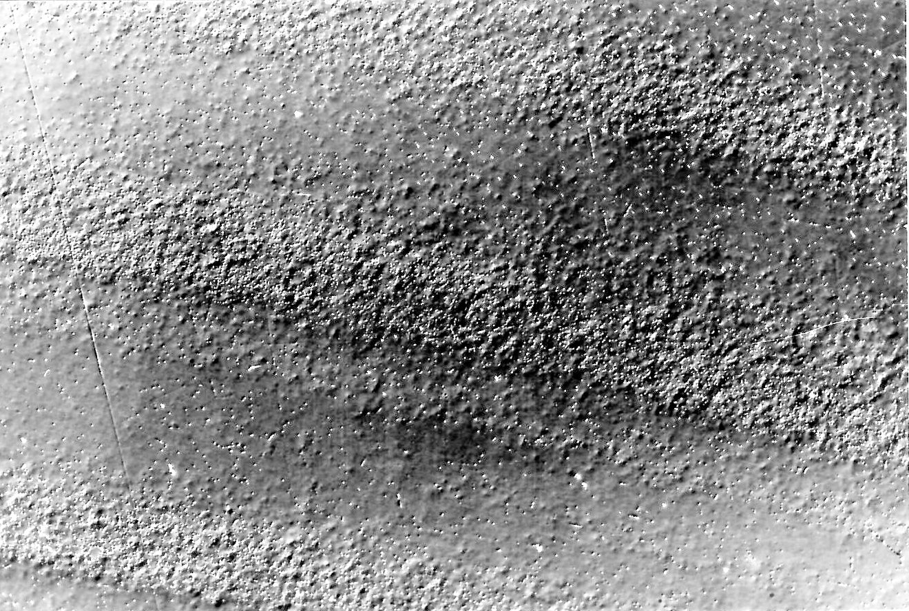 |
"Swirl bands" seen in an optical microscope (using Nomarski interference contrast) at medium
magnification
We have almost exclusively the small B-types swirl defects, producing etch pits. |
|
| |
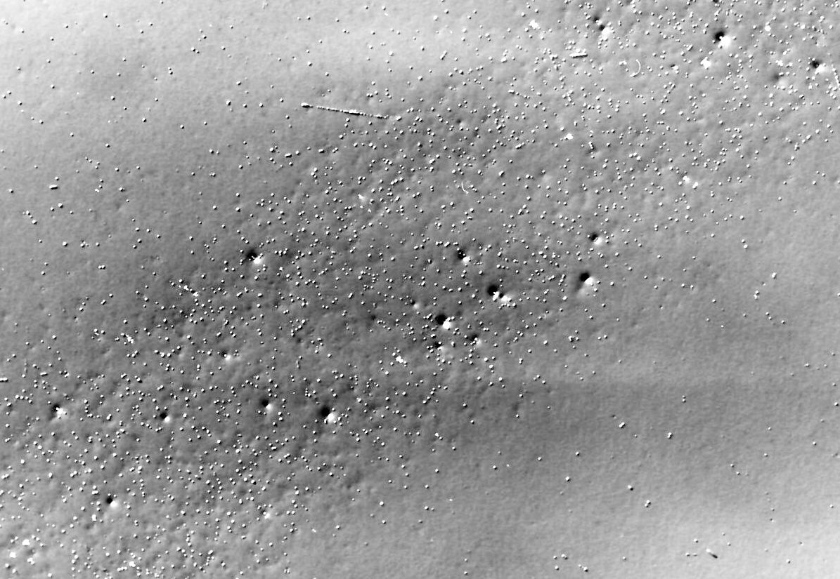 |
Swirl band at high magnification (around 500x) showing big A-swirl hillocks and small B-swirl pits
You can tell hillocks from pits because the "black-.white" vector of changes sign. |
|
| |
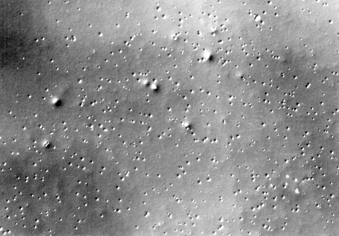 |
| Same as above at higher magnification. |
|
| |
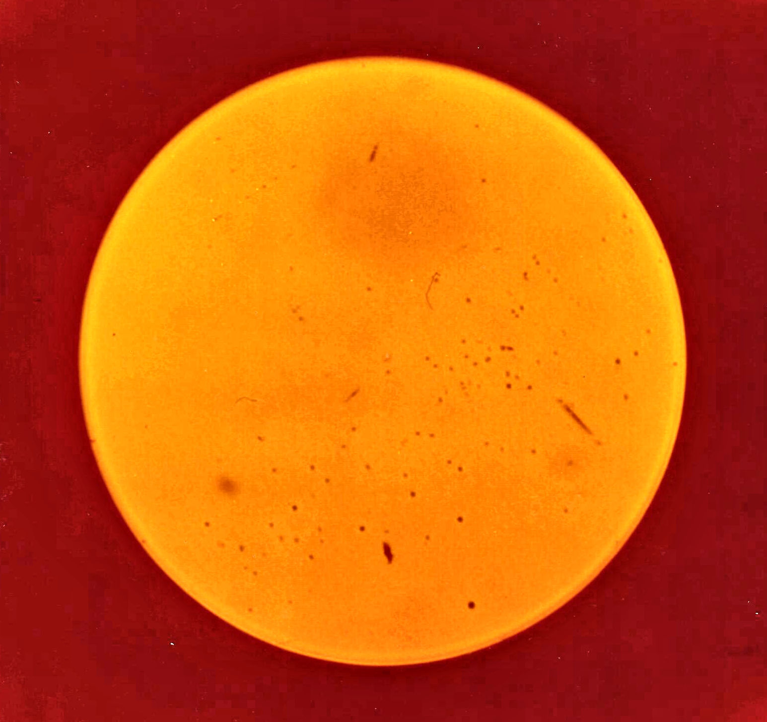 |
Specimen ready for HVTEM inspection. Seen in an optical microscope using through-light..
The
diameter is around 2.3 mm. The thickness of the specimens is around 5 µm and at this thickness Si becomes transparent.
With a HVTEM the whole specimen is transparent (if barely) to the electron beam.
A normally prepared specimen
would only have a small fraction of the whole area transparent to the beam.
The A-swirls are visible as darker spots
since the thickness is larger at the hillocks. Finding one in the HVTEM still could take
a long time
|
|
| |
|
 |
Agglomerates of point defects like vacancies (or interstitials) in a fcc type
crystal like Si should result in small dislocation loops containing a stacking fault
The Burgers vector would be of
the Frank type (b=a/3 {111}. There also could be voids, stacking fault tetrahedra or something else exotic. |
|
 |
As expected, we found discolorations loops containing stacking faults - occasionally.
Some are shown below. They were rather large, however.
As not expected: |
| | |
|
| |
|
All dislocation loops analyzed were
of the
interstitial type!
|
|
| | |
|
|
 |
In part 2 some pictures of the analysis
are shown |
| | |
|
| |
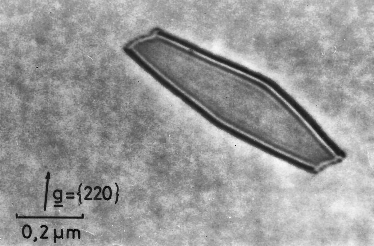 |
| Dislocatpn loop containing a stacking fault. |
|
| |
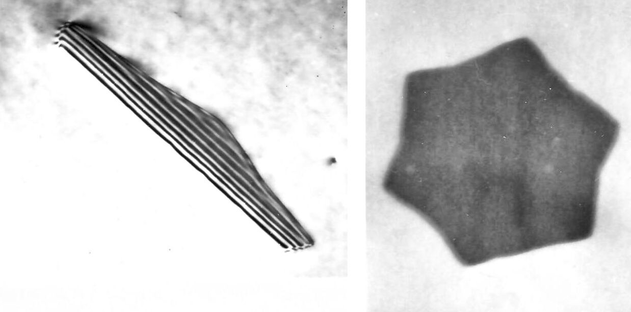 |
Dislocations loops with a stacking fault. Diameters roughly 1 µm
For exact scale and diffraction
vector see the publications.. |
|
| |
|
 |
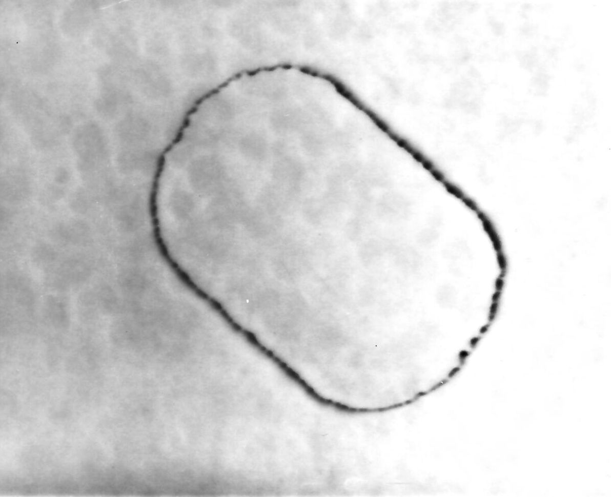
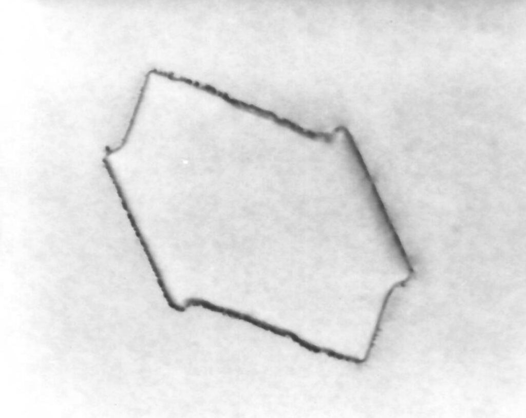
One would have expected "unfaulting" at much smaller diameters but their
might be problems with nucleating the Shockley dislocations needed for unfaulting. Anyway, we certainly did see dislocation
loops without stacking fault that must have resulted form an unfaulting process. The dislocations are now perfect dislocations
that can move as long as the temperature is still high. |
|
 |
Dislocation movement might occur because the dislocation line wants to be straight
in a certain direction or because the dislocation reacts to the stress always there due to temperature gradients |
| | |
|
| |
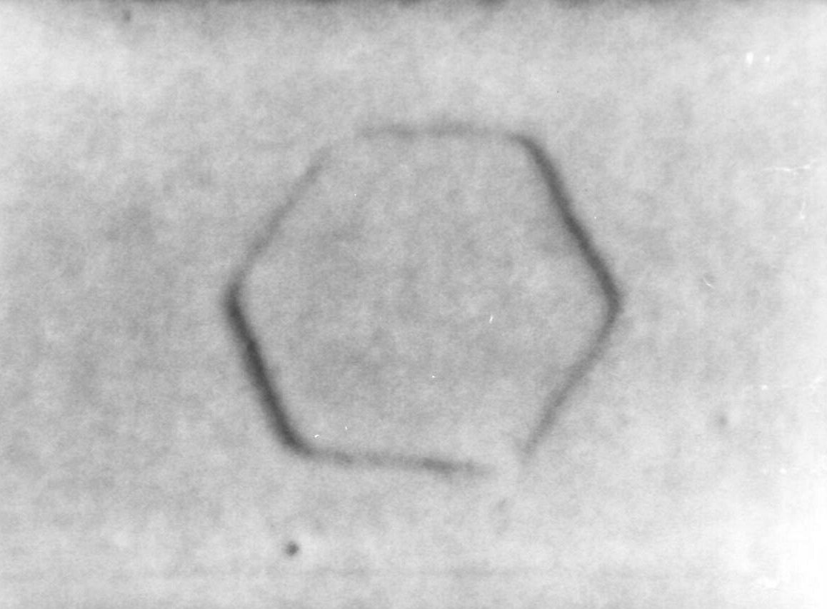 |
| The companion to the hexagonal loop above but with the he sacking fault removed
|
|
| |
 |
| . |
|
| |
 |
| . |
|
| |
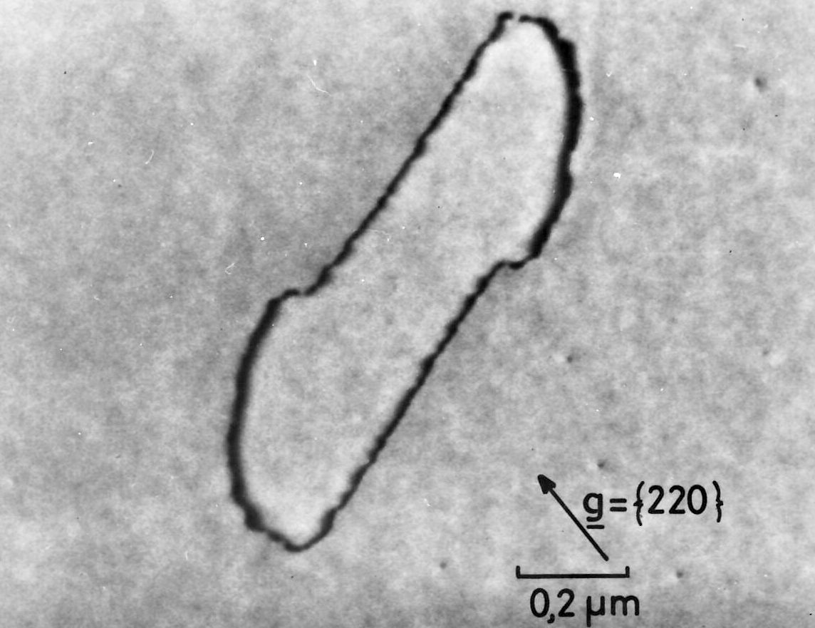 |
| Various single loops just starting some readjustments of their shape. |
|
| |
|
 |
The majority of the A-swirls, however, consisted of more than one dislocations
loop. Here are examples: |
| |
| |
| |
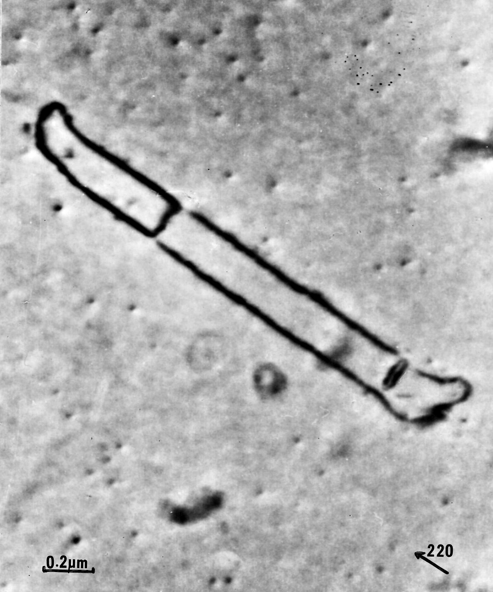 |
| Double loop with a small third loop (or an impurity precipitate ?) attached at one end. |
|
| |
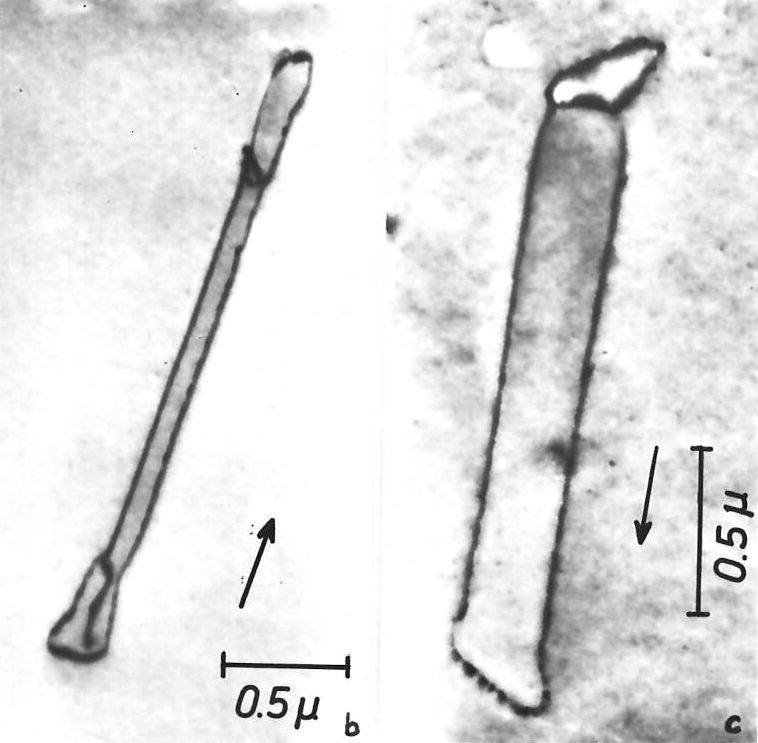 |
| More multi loops. |
|
| |
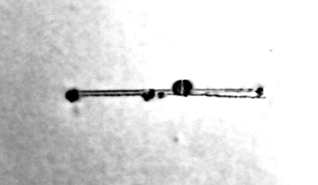 |
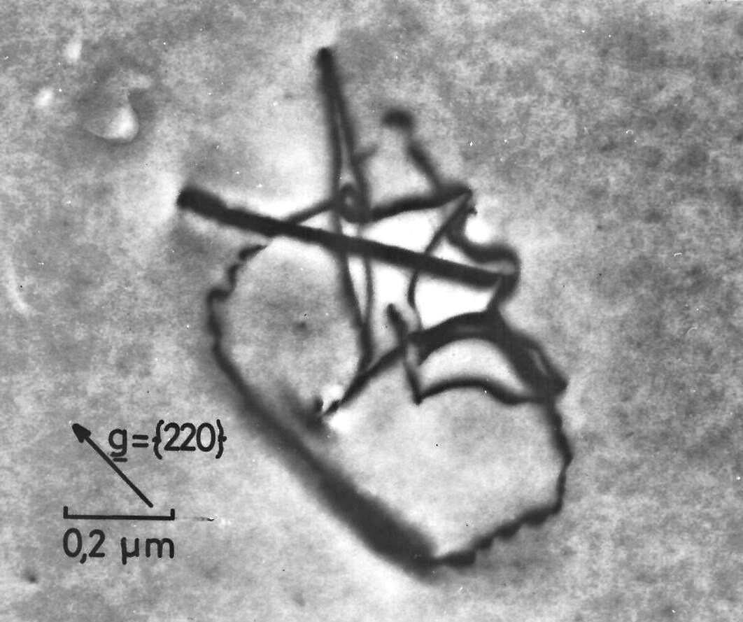
| It becomes clear that the swirl dislocating loops do act as nucleation center for impurity precipitation.
|
|
| |
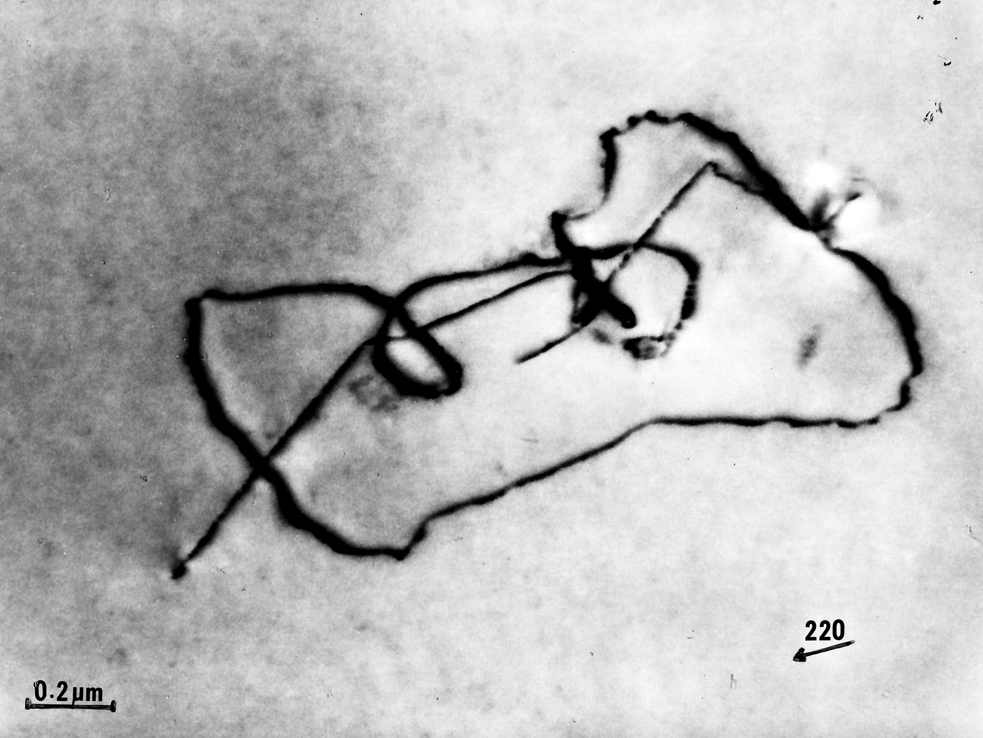 |
| Rather weird structures could be found (and it will get even weirder). |
|
| |
 |
| Another weird one. |
|
| |
|
 |
In a very few cases more complex structures contained still a stacking fault in
parts. This may be taken as a hint that the original nucleation site for an A-swirl defect could nucleate several loops
or dislocation looo – precipitate constructs simultaneously
Here are examples: |
| | |
|
| |
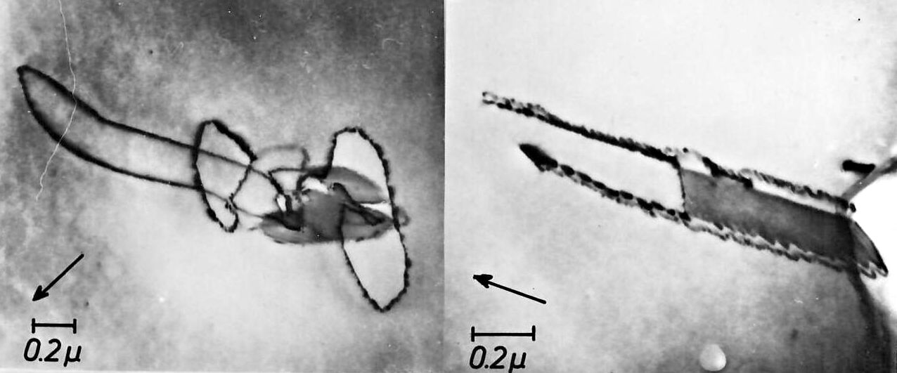 |
| Stacking faults (and precipitates?) in parts of the structure. |
|
| |
|
 |
As far as structural weirdness goes, you haven’t seen anything yet! The show
continues here: |
| | |
|
| |
|
|
| | |
|
 With frame

 2.3 Swirl Defects in Si (Investigated in a HVTEM)
 Pictures to: 2.3 Swirl Defects in Si (Investigated in a HVTEM; Part 2
 Pictures to: 2.3 Swirl Defects in Si (Investigated in a HVTEM); Part 3
© H. Föll (Archive H. Föll)
![]() 2.3 Swirl Defects in Si (Investigated in a HVTEM)
2.3 Swirl Defects in Si (Investigated in a HVTEM) ![]() Pictures to: 2.3 Swirl Defects in Si (Investigated in a HVTEM; Part 2
Pictures to: 2.3 Swirl Defects in Si (Investigated in a HVTEM; Part 2 ![]() Pictures to: 2.3 Swirl Defects in Si (Investigated in a HVTEM); Part 3
Pictures to: 2.3 Swirl Defects in Si (Investigated in a HVTEM); Part 3