|
Pictures to: 2.3 Swirl Defects in Si (Investigated in a HVTEM)
Part 3 |
| |
|
|
|
 |
Months after I thought I was done with archiving the swirl work, I found another
file full of pictures not yet selected. Here is a small number of these finds. |
| |
|
 |
First, a few optical pictures showing the swirl pattern on our 33 mm FZ crystals. The pulling speed is also indicated. |
| |
|
| |
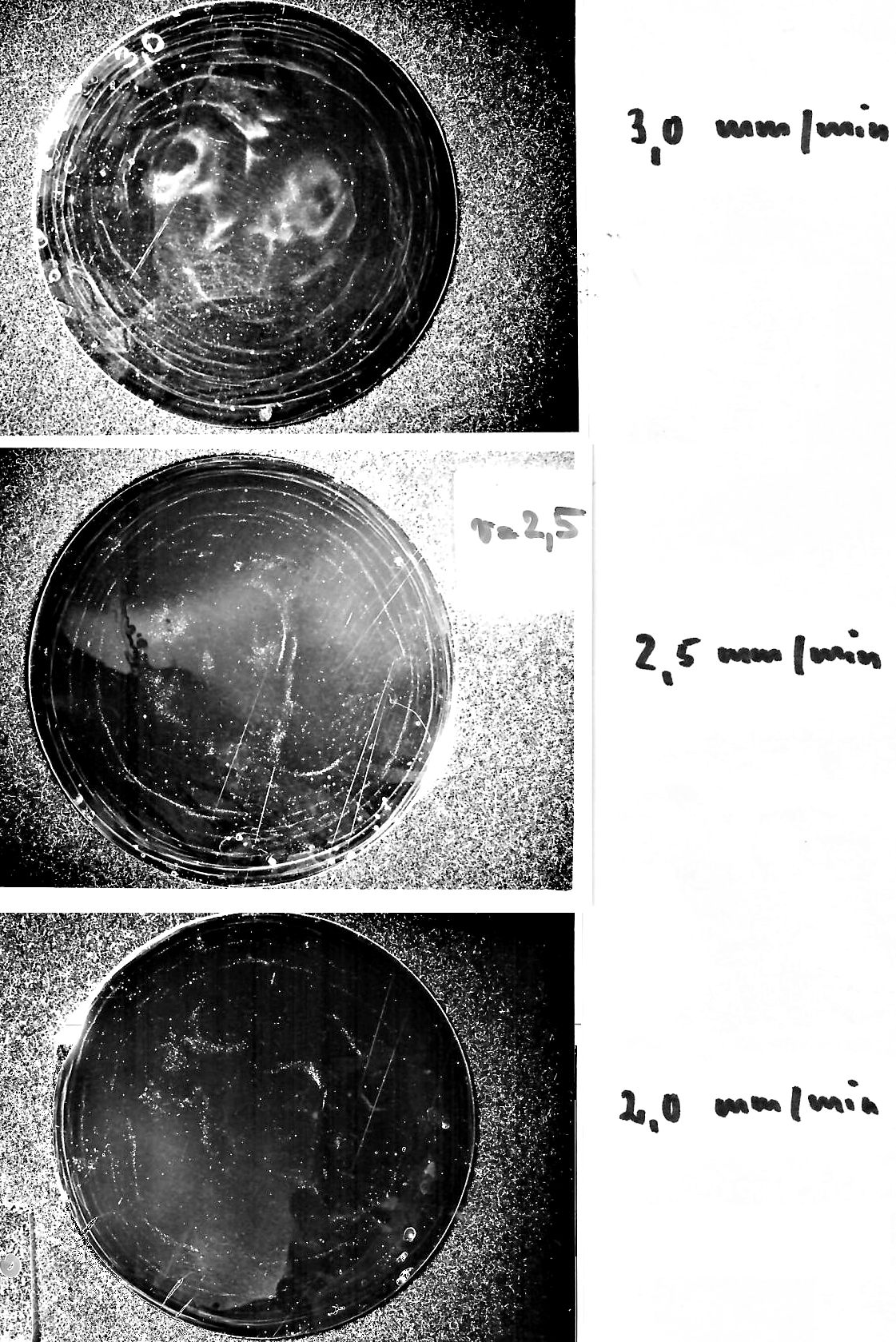
| | Probably <100> oriented |
|
| |
|
| |
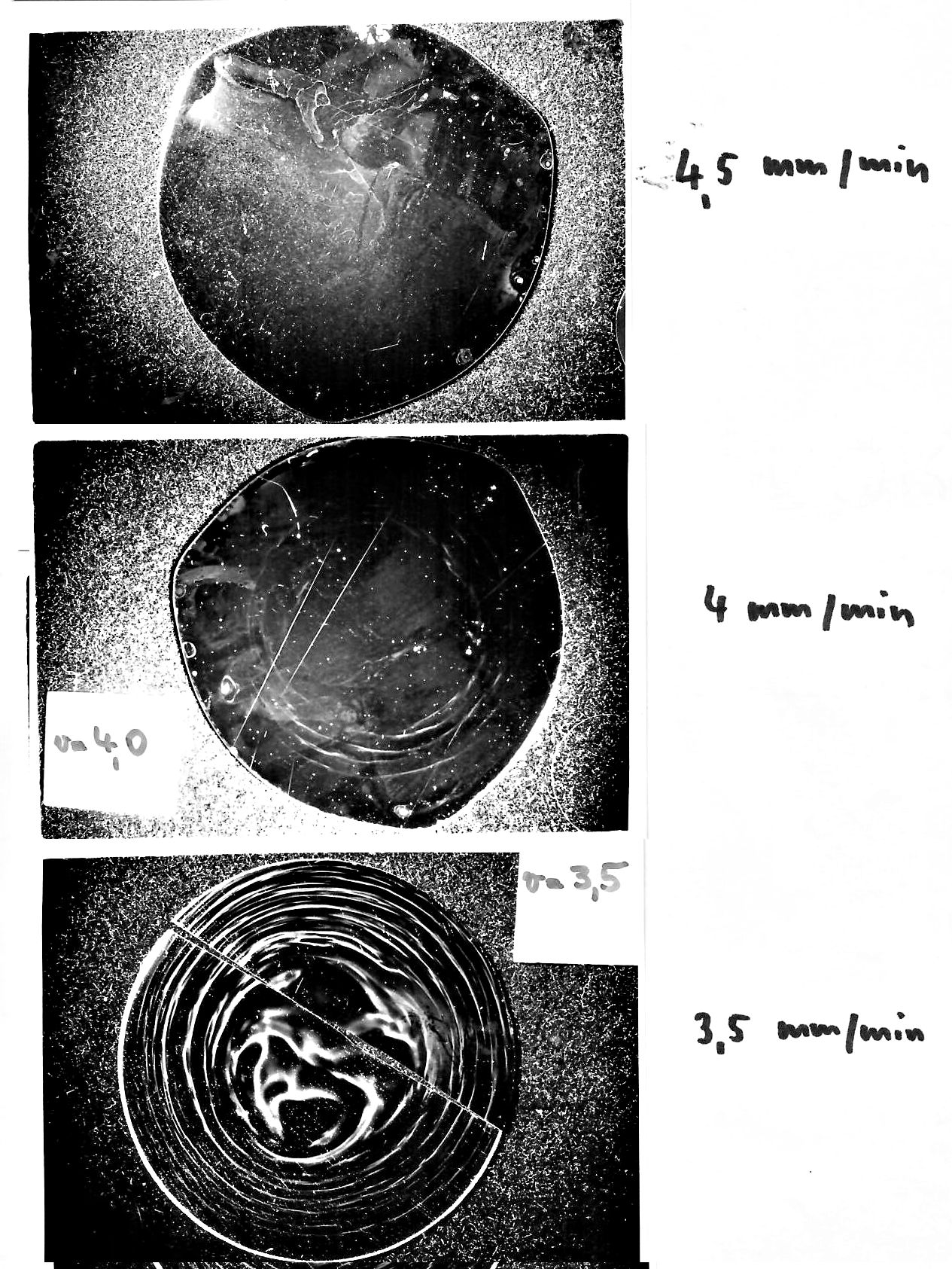
| | Probably 111 >oriented |
|
| |
|
| |
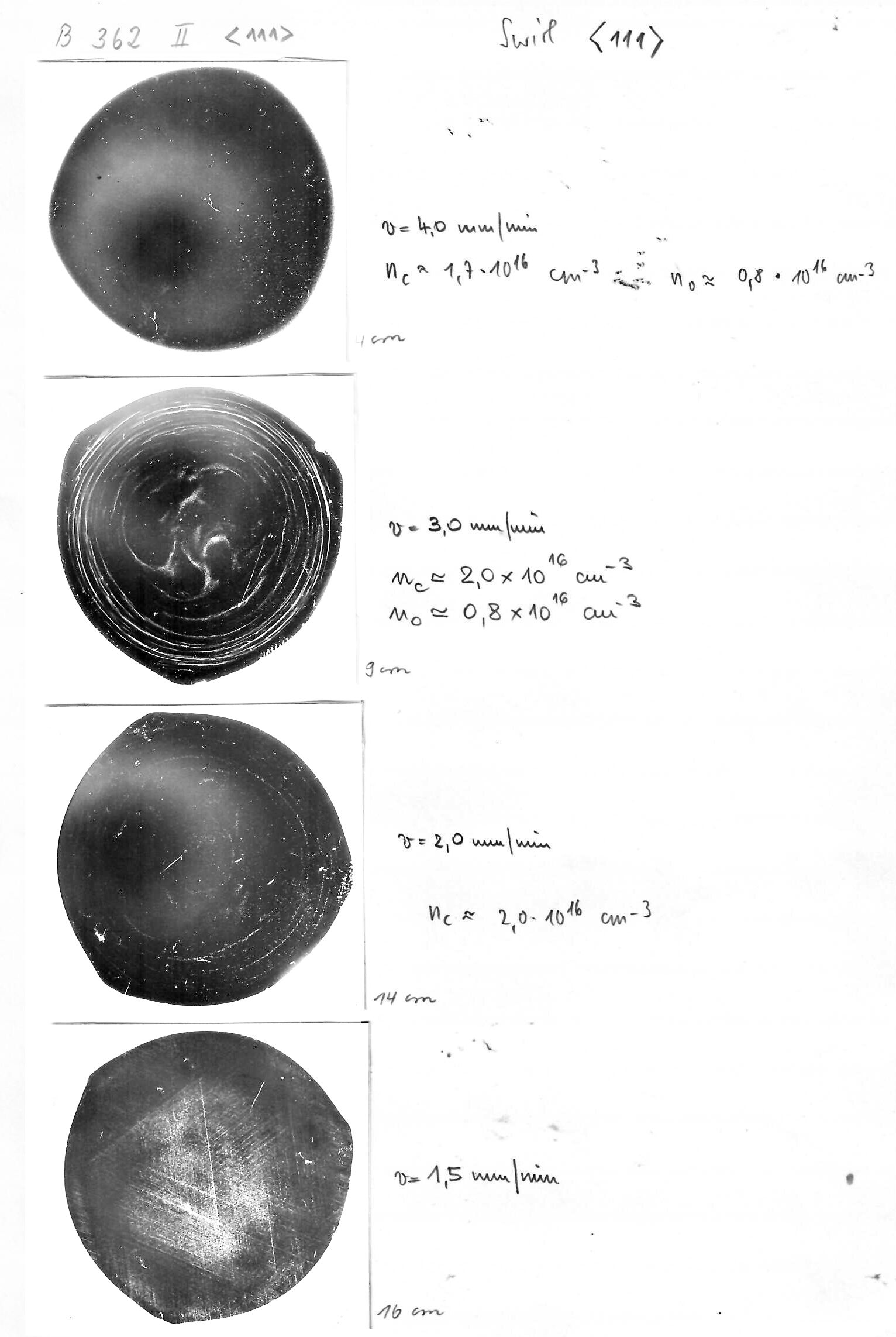
| | At the lowest growth speed dislocations were generated |
|
| |
|
 |
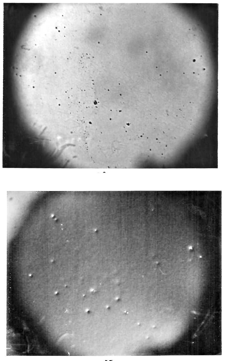
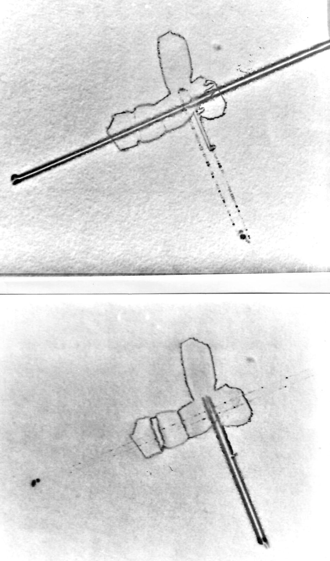
One more example to specimens preparation |
| | |
| |
|
Top: 2.3 mm diamter specimen, though-light view
Bottom: Looking at the surface |
|
| |
|
| |
|
Huge defect shown at two different diffraction conditions.
Here, as in other examples, the very
long and straight dislocations dipoles are
decorated by second order agglomerates. |
|
| |
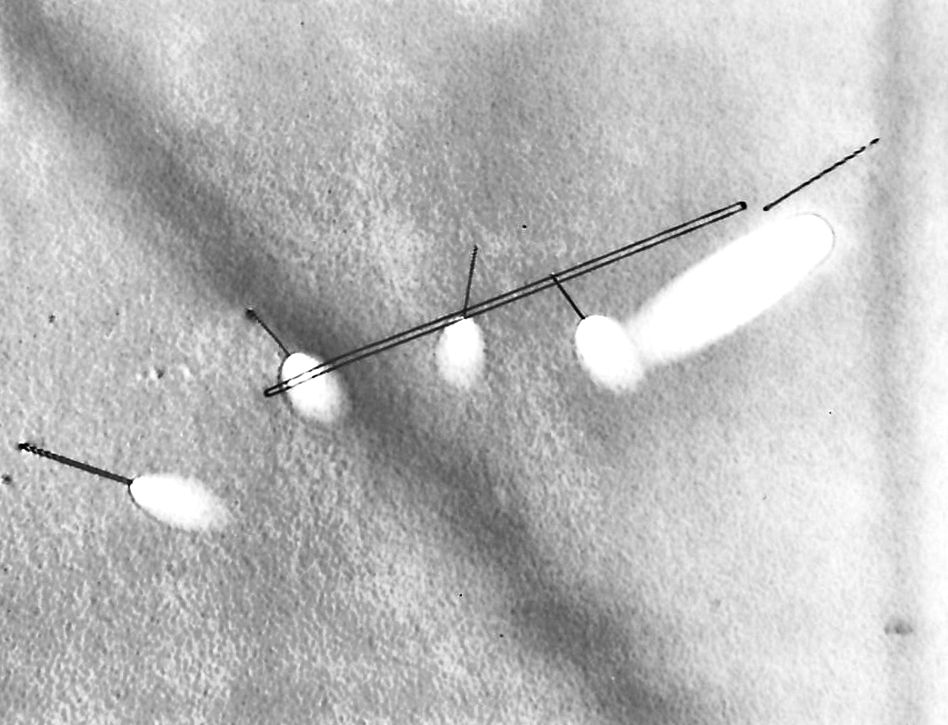
| A rather weird assembly
Of course, the major part of this defect might have been etched out by specimen preparation, witness the etch pits. |
|
| |
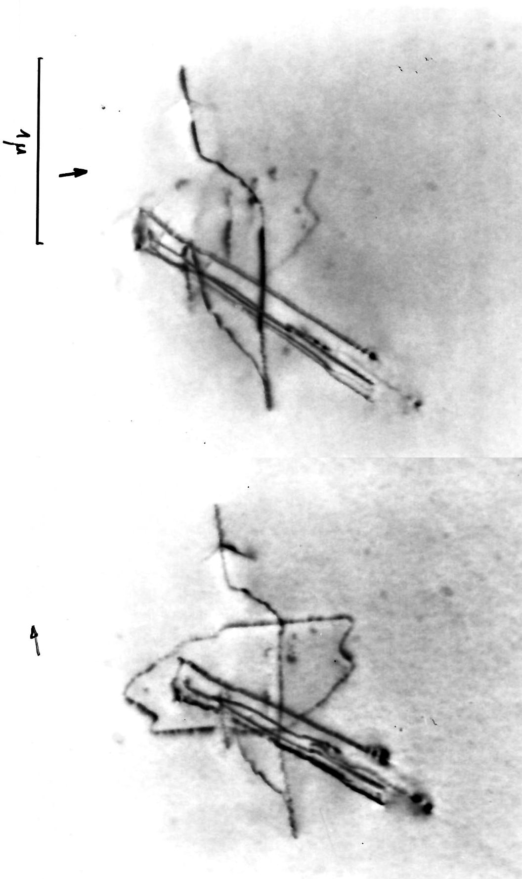
|
Complex defect shown at two different diffraction conditions.
A simple unfaulted loop seems
to be at the heart of the defect.. |
|
| |
|
| |
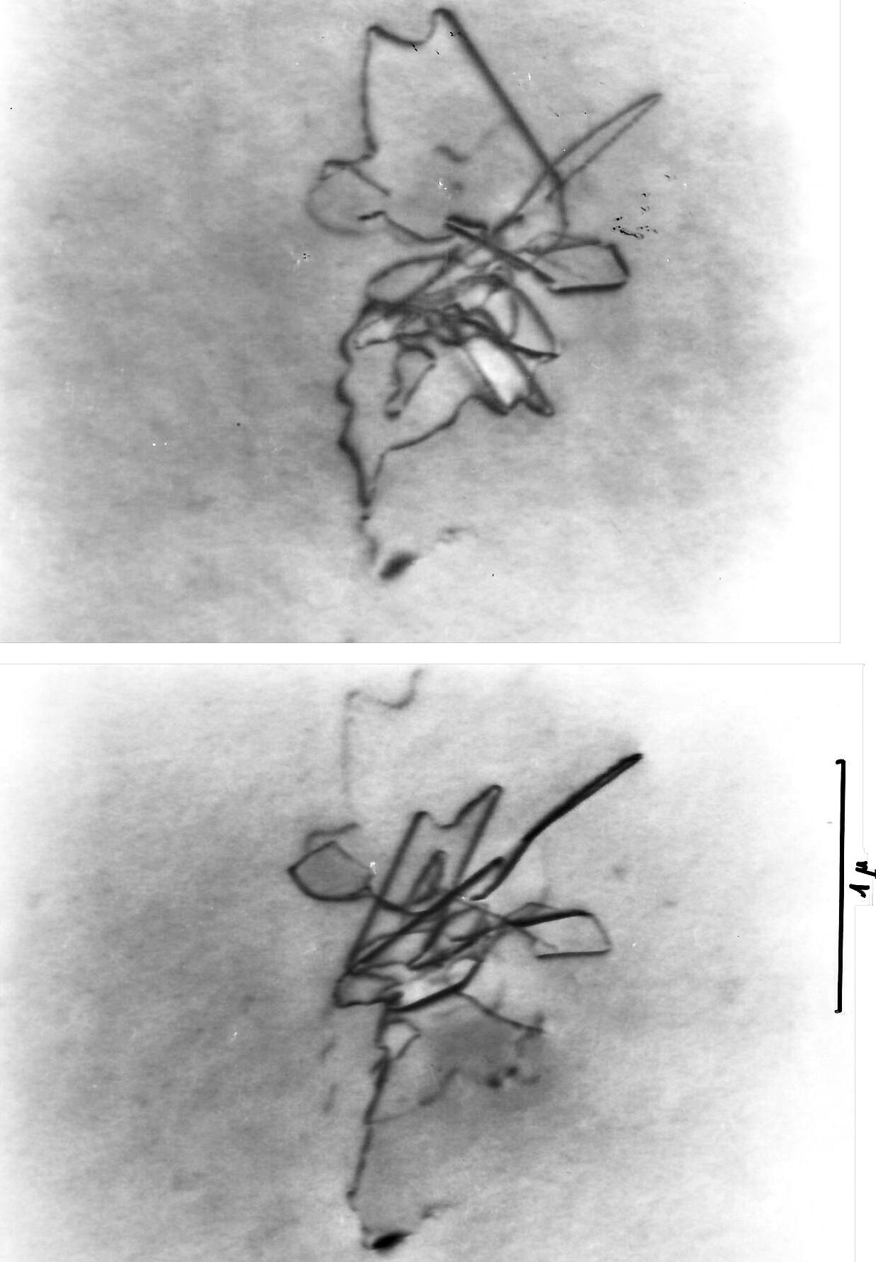
| Complex defect shown at two different diffraction conditions.
. |
|
| |
|
 |
Here are the links to the rest |
| | |
|
| |
|
|
| | |
|
 With frame

 2.3 Swirl Defects in Si (Investigated in a HVTEM)
 Pictures to: 2.3 Swirl Defects in Si (Investigated in a HVTEM; Part 1
 Pictures to: 2.3 Swirl Defects in Si (Investigated in a HVTEM; Part 2
© H. Föll (Archive H. Föll)
![]() 2.3 Swirl Defects in Si (Investigated in a HVTEM)
2.3 Swirl Defects in Si (Investigated in a HVTEM) ![]() Pictures to: 2.3 Swirl Defects in Si (Investigated in a HVTEM; Part 1
Pictures to: 2.3 Swirl Defects in Si (Investigated in a HVTEM; Part 1 ![]() Pictures to: 2.3 Swirl Defects in Si (Investigated in a HVTEM; Part 2
Pictures to: 2.3 Swirl Defects in Si (Investigated in a HVTEM; Part 2