1.2.4.  Research at Siemens in Munich 

Solar Cell Research and Electrochemistry of Silicon
     
  Siemens had decided to start a huge and ambitious program for making cheap but good solar cells. Solar grade Si was to be made cheaply by some process, and with this Si, flat-sheet Si was supposed to be produced by one of various approaches to be investigated. I was to do all the analysis necessary to evaluate the quality of the Si produced. I was also to be the project leader of the S-Web technology in due time. With hindsight I is clear that the project was rather crazy from the very beginning. .
Read the chapter for details.
A key part was a new technique for making thins Si sheets: Take a coarse net woven form purified graphite fibers and pull it through a slot in the bottom of a contained filled with liquid silicon. This is the “supported Web” or S-Web technique. Sound crazy, is crazy – but works!
Not in the way originally conceived but in variants thereof. While this (and other) techniques were developed, there was a constant need to characterize various Si samples produced in some exotic way. For doing this, I introduced my “anodized etching” which lead to a broad investigation of the geochemistry of silicon in general, with far reaching consequences for me and others.
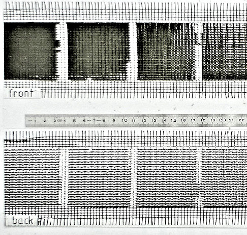
S-Web Siemens
Front (top) and back (bottom) of S-Web
     
ELYMAT
  “ELYMAT” is an acronym standing for "ELectrolYtical MetAl Tracing"
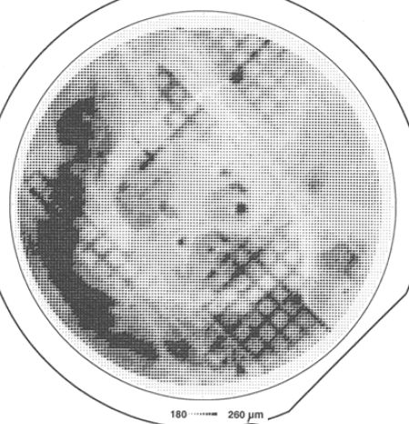
If you introduce tiny traces of sum metal into your Si while processing it, you can just about forget your yield of functioning chips. "Traces" implies, for example, that the Si wafer contacts a pieced of metal just once. Some iron atoms sticking to the Si surface might diffuse into the interior next time the wafer is heated and start to do mischief. In particular, they reduce the minority carrier life time. The ELYMAT technique, a rather elegant if somewhat tricky process, allows precise and local quick measurements of the life time.
It actually generates a life-time map and thus a direct picture of dirt distribution. As the illustration shows, with some luck you see the source of the contamination (here a wafer chuck). The ELYMAT was commercialized and helped to clean up Si processing in many places.
ELYMAT
Early ELYMAT picture showing a life-time map and thus the distribution of amputates
     
Pore Etching
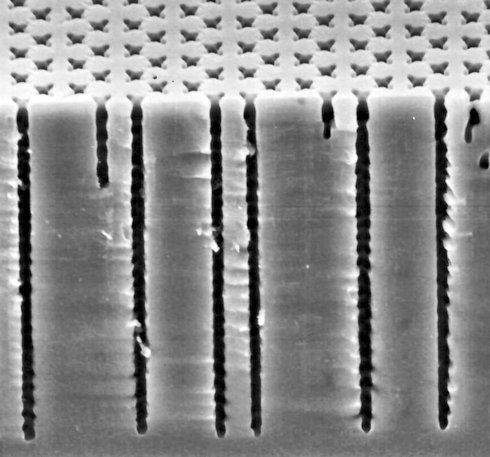
  The picture shows macropores in n-type silicon and is related tot the pictures in my most famous publications No 60.
It opened the doff to thousands of more pictures showing all kinds of pores in several different semiconductors. That is the topic of my second most famous publications No. 135.
No more needs top be said.
First macropores in Si
The very first macropores etchanodically ed into silicon
     
Microchip Development
  It is impossible to describe the excitement and stress of being engaged in the development and a new microchip. I could experience this unique atmosphere for several years, in the end as project leader of the 16Mbit DRAM. I tried to impart a flavor of this kind of work in publication No. 61
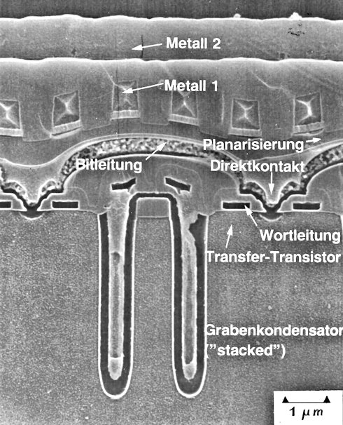
The picture show a SEM picture of a cross-section: I certainly did not “make” the chip (that took a dedicated bunch of 1 few 100 people) but I was in charge of the SEM (and other) analytics.
Cross section DRAM
Cross-section through 18 Mbit DRAMSEM
     
Links to:
  Chapter 2: Chapter 2: Early TEM Work in Stuttgart
  Chapter 3: TEM Work at Cornell University
  Chapter 4: Research at IBM T.J. Watson Research Center
  Chapter 5: Research at Siemens in Munich
  Chapter 6: Research at the Christian-Albrechts-Univesität zu Kiel
  Chapter 7: Hyperscripts and Teaching in Kiel
 

With frame Back Forward as PDF

© H. Föll (Archive H. Föll)