1.2.3. TEM and Other Work at IBM Research

|
1.2.3. TEM and Other Work at IBM Research | |||
| TEM Investigations of Silicides |
|||
| Silicides, i.e. metal-Si compounds, were deems important for the future of microelectronics at the end of the 1970ties. You could either sputter them on or form them by a solid state reactions with the Si. The idea was to study their formation by coating silicon with some metal followed by some annealing. A silicide forming reaction could occur because the metal diffuse into the Si, eventual forming the most Si-rich silicide found in the phase diagram, or Si diffusing into the metal producing the metal - rich silicide. Continuing heating (and possibly increasing the temperature) would produce all the other silicides the phase diagram provided, i.e. Ni2Si, NiSi and NiSi2. Or things were different from this simple view of silicide formation. Thing actuality were different on occasion. That much was known but there was still lots of room for a detailed investigation. I looked at the Pd-Si, Pt-Si and Ni-Si system. I took the very first HRTEM picture of a heterogeneous interface (the picture on the right) and a lot of other spectacular micrographs, providing a lot of new insights. |
| ||
| TEM of Defects Produced by Ion Implantation | |||||
| s | |||||
| Implantation Damage 1 (AS, 80
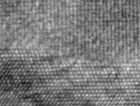
keV) Ion implantation was a rather new technology in 1980 and the damage produced in the silicon crystal by shooting high energy ions into it, possibly with high beam intensities, was of considerable interest. Weird things were known to happen. Like the amortization of a surface layer and in particular the formation of some planar defect on {113} planes. It appears that I took the very first high resolution pictures of ion implantation induced defects, the picture on the right shows an {113} defect on top and the boundary between amorphous and crystalline Si at the bottom half. Colleagues saw a lot more interesting stuff in those HRTEM pictures and wrote a string of publications. Much work has been done since then, and beautiful HRTEM images with much better resolution than mine were produced. IN the main part I give you a few references. Nevertheless, there are still plenty of open questions. The structure of Sdi self-interstitials under various circumstances and what they do if present in supersaturation proved to be far more complicated than we could imagine the |
| ||||
| Anodic Etching of Defects in Si |
|||||
| Starting some really stupid experiments while waiting for TEM time, I discovered by accident anodic defect etching in p-type silicon. Running current through (poly-crystalline) samples either etched all defects or only the electrically active ones, depending on settings. The quality of the etching was as good or better than standard chemical defects etches. The picture (top to bottom) shows anodic defect etching on the “only electrically active defects” mode, and EBIC (electron induced current) picture that by definition shows only electronically active defects, and a standard chemical defect etch (“Sirtl”). What happens is rather clear (in hindsight), just look at a somewhat involved junctions theory for IV characteristics. That work had unexpected and rather far reaching consequences. I used (and expanded) the technique extensively in the Siemens solar energy project (see chapter 5) and it started me on the electrochemistry of semiconductors in general, a topic that I pursued for many years to come and where I could make major contributions. |
| ||||
© H. Föll (Archive H. Föll)