1.2 Overview of Content


1.2.1. : Early TEM Work in Stuttgart

Elektronenmikroskopische Untersuchung der Strahlenschädigung in ionenbestrahlten Kobalt-Einkristallen (Chapter 2.1)
Electron Microscope Investigation of the Damage in Cobalt Single Crystals Introduced by Ion Irradiation
  My Diploma Thesis work, in other words.
Bombard Co specimen already prepared for Transmission Electron Microscopy (TEM) with gold ions having an energy around 60 keV and then use a TEM to see what kind of damage that produced.
Straight forward except for:
  • Specimen preparation was more tricky then envisioned. You also learn that TEM work is 90 % specimen preparation and not looking on some screen.
  • Co is ferromagnetic and thus disturbs the magnetic field of the objective lens. That needs major realignments of the instrument (especially astigmatism) and makes it hard to obtain good crisp pictures.
  • The damage produced (small dislocation loops) is too small to be seen directly with the 1970th TEMs. You thus produced "black-white contrasts" that gave indirect images and needed major theory for interpretation.
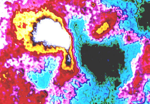
Ion irradiation damage in Co
  The picture shows a special "black-white" contrast (getting close to a so-called "butterfly). The original grey levels have been replaced by color in a (then) rather tricky and time-consuming process., done by me for the first time; I believe.
     
Agglomerate Atomarer Fehlstellen in Silizium - Part 1 (Chapter 2.2)
(Low Temperature Electron Irradiation Damage)
Agglomerates of point defects in Si
  My Ph.D. Thesis. It consists of two parts. Here is part 1 (actually written as the second part in the paper but my original starting point):
High-Voltage TEM (HVTEM) Investigation of In-Situ Electron Irradiation Damage in Si at Low Temperatures
Keep a Si specimen (necessarily rather thin) in a HVTEM operated at 650 keV at low temperature (down to 20 K) and watch what happens.

Well - not a lot happens. But what happens is rather complicated and depends on many more parameters then in metals.
It appears, for example, that "shot-in" impurity atoms act as nucleation centers for small agglomerates of something (probably interstitials). This implies that the visible damage appears close to the "upper" surface, which is indeed what one finds (with difficulties).
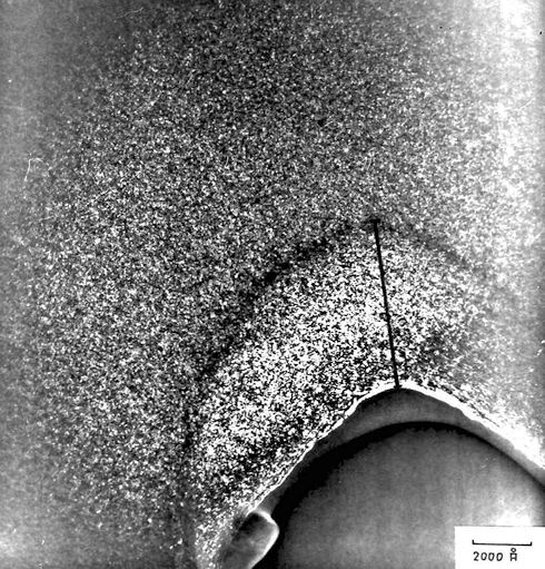
Low T irradiation Si
  Along the black line in the picture the specimen thickness decreases from its "bulk" value to zero (we have an etch pit there). The density of defects (white "points"), however stays the same. The brightness of the "points" increases because the specimen gets thinner, but not the density.
The defects are close to the surface, in other words.
   
Agglomerate Atomarer Fehlstellen in Silizium - Part 2 (Chapter 2.3)
(Swirl Defects in Float-Zone Si Crystals)
Agglomerates of point defects in Si
  My Ph.D. Thesis once more. Here is the second part:
High-Voltage TEM (HVTEMI) investigation of Swirl Defects in FZ Si
Pull an ultra-clean and dislocation-free Si crystal with the float-zone (FZ) method and you will find that it still contains a few tiny defects called swirl defects in reference to their spatial distribution. All and sundry assumed that these swirl defects must be agglomerates of vacancies. After all, at a temperature right below the melting point the crystal supposedly contains a "high" concentration of vacancies in thermal equilibrium. As the temperature decreases, the equilibrium concentration of these vacancies decreases exponentially and this implies that the surplus vacancies must disappear. If no "big" defects like dislocations or grain boundaries are around that could act as sinks, the vacancies need to cluster into, for example, small dislocations loops. Perfectly straight-forward thinking, experimentally verified in many (metal) cases.
Small dislocations loops is what we found. However - they originated by agglomeration of Si self-interstitials and not vacancies!
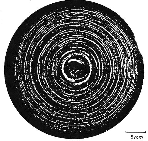
Swirl defects in Si
 
  We thus claimed that in Si self-interstitials and not vacancies are the dominating equilibrium point defect and thus committed a the equivalent of a sacrilege. Interesting times followed.
The picture shows the etched surface of a Si wafer with the swirl defects showing as white dots. It illustrates nicely why those defects are called the "swirls"
   
Process Induced Defects in Integrated Circuits (Chapter 2.4)
  Work done "on the side" by Bernd Kolbesen (and a Siemens background crew) and me while I worked for my thesis. It could have been part of my thesis, too, but three independent parts would have overtaxed the system. You were supposed to be single-minded,
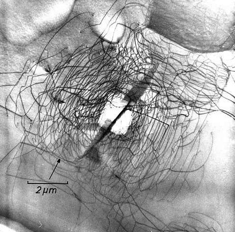
Process induced defect in Si
 
  This work rested on a superior specimen preparation technique of the Siemens people (mostly ....) that allowed to prepare a specimen that was thin enough to be investigated by a HVTEM over the whole specimen area (about 2 mm2). And this enabled us to look into parts of integrated circuits that didn't work properly as ascertained by measurements prior to specimen preparation.
We could thus correlated process-induced crystal lattice defects to local failure. Figuring out how these defects came into being helped to figure out how to avoid them. A rather big and important topic for the whole (then still rather small" industry.
  The picture show a dislocations tangle most likely produced by indenting the surface somehow (a probe?). A very small pit plus a microcrack was produced that, upon the fist heating cycle, started to emit dislocations that in turn "killed" the transistor that contained them
   
Links to:
  Chapter 2: Chapter 2: Early TEM Work in Stuttgart
  Chapter 3: TEM Work at Cornell University
  Chapter 4: Research at IBM T.J. Watson Research Center
  Chapter 5: Research at Siemens in Munich
  Chapter 6: Research at the Christian-Albrechts-Univesität zu Kiel
  Chapter 7: Hyperscripts and Teaching in Kiel
 

With frame Back Forward as PDF

© H. Föll (Archive H. Föll)