 |
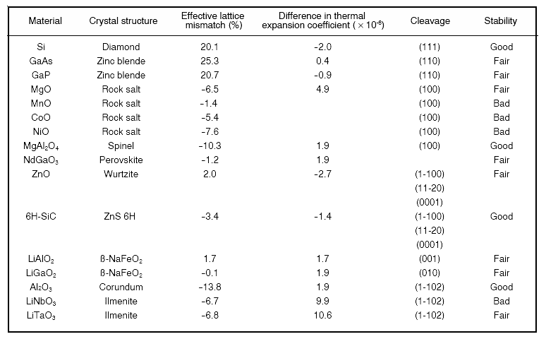
The module is based on the paper of Kuramta et al: in FUJITSU Sci. Tech. J. 342
(1998). p.191. The authors provide data about cleavage planes in semiconductors.
|
|
 |
The preferred cleavage planes of a semiconductor are not as clear-cut as it seems.
As everybody know who just once dropped a {100} Si wafer knows, the fracture plans are the {110} planes; a
large part of the literature, however, including the paper given above, insists that it should be {111}. |
|
 |
Be that as it may, here we take the planes given in the article. |
| |

From the Ref. given above
Comparison always to GaN |
|
 |
GaN as a semiconductor technology material only comes as a thin layer on
a substrate other than GaN since there simply are no usable GaN
single crystals |
|
 |
As we know, if we grow thin layers with different lattices, we have to watch
out for misfit dislocations. It is important to look for substrates
with a lattice constant as similar as possible to that of the thin layer to be grown. The table above shows the lattice
mismatch of prospective substrates to GaN and thus gives a guideline. |
 |
If we want to make a Laser diode form the thin film, we have a few more requirements
besides "just" avoiding misfit dislocations as best as we can: |
|
 |
The substrate should have a high electrical and thermal conductivity. The first
property would make it easier to supply the large current densities we need to operate a Laser diode, the second to remove
efficiently the heat generated during operation. |
|
 |
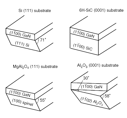
The whole stack of substrate and layers should cleave nicely on a well-defined
and very flat plane because the two relevant surfaces obtained by cleavage will serve as the mirrors of the Faby-Perot resonator we need for a Laser. Now look at the possible cleavage relations: |
| |

From the Ref. given above |
|
 |
Summing up: There is no ideal substrate - you have to find the optimal compromise
once more if you wan to make the blue Laser diode. |
| |
|
© H. Föll (Semiconductor Technology - Script)

