 |
A solar cell converts light power into electrical power. It's overriding parameter
is the over-all conversion efficiency h |
|
Important "raw" numbers.
- Maximum h Si solar cell » 25 %
- Maximum sun power » 1 kW / m2.
- Maximum commercial solar cell power » 200 W / m2.
- Yearly average commercial solar cell power » 25 W / m2.
|
| Solar cell science and technology centers exclusively on money
and saving the earth! |
 |
| h | = |
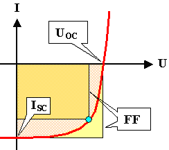
const · UOC · ISC· FF |
|
|
|
 |
Any solar cell is essentially a large -area junction, usually of the pn-type. |
|
|
 |
It's essential parameter are the short-circuit current ISc, the open-circuit
voltage UOC and the fill factor FF |
|
|
 |
For optimal efficiency the bandgap Eg should be matched to the solar
spectrum; we need around 1.5 eV. | |
|
 |
Maximum efficiency from the semiconductor physics point
of view is achieved if all light with energy >=Eg produces minority carriers and all
of these carrier are swept out as diode reverse current and |
|
|
 |
Maximum efficiency from the module systems point of view
is achieved if the semiconductor part is OK, only very little light is reflected by the solar cell module, series
resistances and shunt resistances can be neglected, and everything is uniform and homogeneous |
|
|
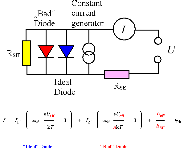
The equivalent circuit diagram with the basic equation has is all! |
|
|
 |
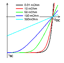
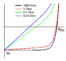
Series and shunt resistances, unavoidable for large areas, are of overwhelming importance
for solar cells with h <» 10 % |
|
| |
| |
|
|
|

Effect of series resistance |
| |
| |
| |
|
|
|

Effect of shunt resistance |
| |
| |
| |
|
 |
Switching solar cells with individual characteristics in series and / or in parallel
causes all kinds of problems. | |

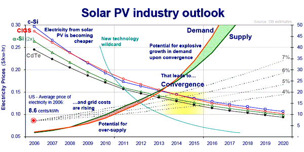
Courtesy Deutsche Bank |
|
|
 |
Worse: Any inhomogeneous solar cell (e.g. mc-Si solar cells) consists of locally
different solar cells "somehow" connected internally |
|
|
 |
Optimizing solar cells with respect to "money" thus provides exciting science and
engineering!
| |
 |
There are many competing solar cell technologies and materials.
- Bulk single-crystal and mc Si vs. thin film Si (a-Si:H, µc-Si:H. ..
- Other thin-film semiconductors:CIGS, CdTe, ...
- Exotica: TiO2- electrolyte ("Grätzel cell"), organic semiconductors, "Nano"
materials, ...
| |
| | |
| |
 |
Bulk Si solar cells are made from (cheap) single crystalline wafers (cut
squarish) or from square multicrystalline (mc) wafers. They account for about 85 % of the installed solar power at present (2008).
| |
| Processing Time |
1s / solar cell |
| Cost Decrease | 5 % / a |
| Efficiency Increase | 20 % in 2012 ? |
| Key Material Supply | 30 % /a more Si |
Industry Growth Rates
> 30 % for many years |
Supply capital and people |
|
|
 |
A yearly production of 1 GWpeak means about 107
m2=10 km2 pn-junction of good quality and much more |
|
|
 |
Consider Þ |
|
|
|
A big problem is cranking up world wide Si production by 30 % - 40 %
per year. | |
|
| |
| |
 |
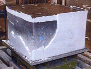
mc wafers are produced by Si casting. Problems are |
|
|
|
 |
Expansion upon crystallization. |
|
|
 |
Reaction with walls of mold | |
|
 |
Columnar grain growth required |
|
|
 |
300 kg ingots are routinely cast in 2007; liquid encapsulation and precise temperature
control are essential | |
 |
Sawing the ingot into mc-Si wafers with as little losses as possible and
with wafer thicknesses of < 300 µm, while straight-forward, is "high-tech". |
|
|
 |
Saw damage is removed by a chemical etch. |
|
| |
| |
| |
 |
Processing, simple in principle, has to meet the conditions above and is highly
specialized. Essential processes are: | |
|
|
 |
Diffusion, edge isolation, passivation, screen printing contacts and sintering contacts. |
|
|
 |
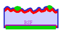
Essential device features are back surface field, gettering of impurity atoms, H-passivation
of grain boundaries and other defects. | |
| | |
| |
 |
Thin film solar cells need to meet some key requirements: |
|
 |
 | | CIGS | Multi junction |
|
|
 |
- Process-compatible and cheap substrate Þ large area deposition.
- Suitable direct band gap Þ high absorption coefficients f
- Insensitivity to "defects"
- Technology for junction and good ohmic contacts.
|
|
 |
Major contenders in (or close) to production are: |
|
|
 |
- Amorphous Si.
- Nanocrystalline thin film Si.
- Polycrystalline thin film Si.
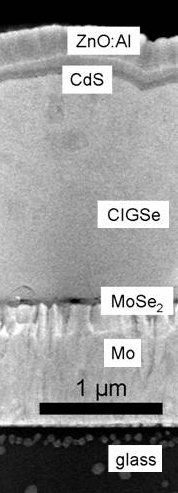
- The CuInxGa1-xSe2 or "CIGS" family.
- The CdTe solar cell.
- May others in R&D
| |
|
 |
The present "high potentials" are CdTe and CIGS. |
|
| |
| |
|
 |
High-efficiency multi-junction solar cells may find applications as "concentrator
cells" at the focus point of a large mirror or lens that tracks the sun. |
|
|
| |
| |
 |
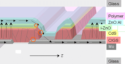
CIGS and most other thin film solar cells have high internal resistances
and need to be switches in series after about 1 cm for high performance |
|
|
|
 |
This must be done automatically and in-situ as part of the production process. |
|
|
 |
A whole new technology needs to be developed for thin film solar cell mass production |
|
 |
The race between bulk Si solar cells and thin film technologies is open
in 2008; the winning technologies are to be determined. |
|
|
| |
|
 |
Solar cells have a bright future! |
| |
| |
|
© H. Föll (Semiconductor Technology - Script)
