 |
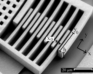
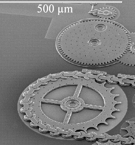
MEMS are "Micro Electro Mechanical Systems" including also micro
optics, micro fluidics and generally meaning micro systems. | |
|
|
 |
MEMS uses Si substrates and technologies because "it is there
and cheap" for the non-electronic part and because electronic components can be
integrated on the same chip. | |
|
 |
Examples of high-volume MEMS products are - (Pressure) sensors.
- Accelerometers.
- Gyros
- "Beamer" chips (DLP)
|
|
|
 |
More products are to come; MEMS is an emerging
and often an enabling technology |
|
 |
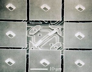
Gyros are particular complex MEMS sensor products with a huge range
of applications. | |
|
 |
There must be a physical principle behind the sensor design; different approaches can be used. |
|
|
 |
One approach uses the Coriolis force causing detectable additional vibrations in an
oscillator with two degrees of freedom if some rotation is experienced. |
|
| |
| |
| |
 |
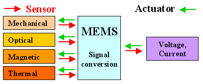
Many MEMS devices are either sensors or actuators. |
|
|
|
 |
Looking only at mechanical MEMS, there is a need to couple mechanical movements to
electrical signals and vice verse. | |
|
 |
Ways to do this include. - Capacitive coupling
- Piezoelectric and piezoresisitive coupling.
- Thermal coupling (expansion, resistivity changes).
- Magnetic coupling.
- Optical coupling.
|
|
|
 |
There is no "ideal" coupling; all methods suffer from certain problems. |
|
| |
| |
|
 |
MEMS uses all of "known" Si technology and has some specifics
of its own. | |
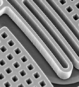
Works |
Sticks |
|
|
 |
Making cantilevers and membranes necessitates making "large" cavities. |
|
|
 |
Staying absolutely planar and stress-free is essential |
|
|
 |
Packaging can be far more demanding than for chips (e.g. transparent tops for OMEMS,
keeping defined pressures for > 10 a in gyros). | |
 |
The bane of MEMS is stiction. |
|
|
 |
If you can't lubricate, it will stick sooner or later.
Never bring moving parts in contact! | |
|
 |
MEMS design therefore cannot just miniaturize exiting mechanical designs; it must look
for new approaches. | |
| | |
| |
 |
MEMS employs some special processes and materials; they are the drivers
of progress | | |
|
 |
Anisotropic chemical etching | |
Making "large" cavities and extremely deep "holes"
Planarization
Free-standing structures |
|
|
 |
High-rate plasma etching ("Bosch process") |
|
|
 |
Chemical-mechanical polishing | |
|
 |
Sacrificial layers and removal (including chemical etching with "vapors") |
|
|
 |
Wafer bonding; in particular for packaging. |
|
|
| |
| |
 |
Process integration looks simple if compared to an advanced CMOS process,
but is actually rather involved due to the special processes needed and quality requirements |
|
|
| | |
|
© H. Föll (Semiconductor Technology - Script)
