 |
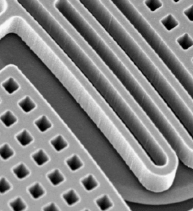
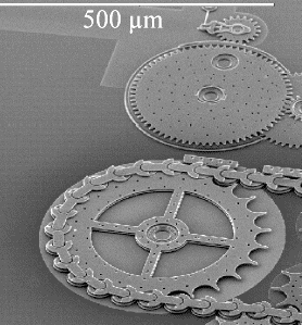
MEMS uses all of "known" Si technology and has some specifics
of its own. | |

Works |

Sticks |
|
|
 |
Making cantilevers and membranes necessitates making "large" cavities. |
|
|
 |
Staying absolutely planar and stress-free is essential |
|
|
 |
Packaging can be far more demanding than for chips (e.g. transparent tops for OMEMS,
keeping defined pressures for > 10 a in gyros). | |
 |
The bane of MEMS is stiction. |
|
|
 |
If you can't lubricate, it will stick sooner or later.
Never bring moving parts in contact! | |
|
 |
MEMS design therefore cannot just miniaturize exiting mechanical designs; it must look
for new approaches. | |
| | |
| |
 |
MEMS employs some special processes and materials; they are the drivers
of progress | | |
|
 |
Anisotropic chemical etching | |
Making "large" cavities and extremely deep "holes"
Planarization
Free-standing structures |
|
|
 |
High-rate plasma etching ("Bosch process") |
|
|
 |
Chemical-mechanical polishing | |
|
 |
Sacrificial layers and removal (including chemical etching with "vapors") |
|
|
 |
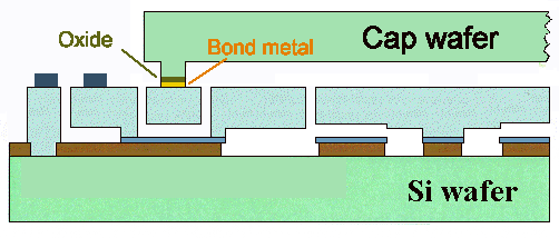
Wafer bonding; in particular for packaging. |
|
|
| |
| |
 |
Process integration looks simple if compared to an advanced CMOS process,
but is actually rather involved due to the special processes needed and quality requirements |
|
|
| | |
|
© H. Föll (Semiconductor Technology - Script)
