 |
Silicondioxide (SiO2) has been the "ideal" dielectric
with many uses in chip manufacture | |
- Gate oxide for Transistors
- Dielectric in Capacitors
- Insulation
- Stress relieve layer
- Masking layer
- Screen oxide during Implantation
- Passivation
|
|
|
 |
Only recently (2007) is it replaced by "low k"
and "high k" dielectrics, i.e. dielectrics with a dielectric constant either lower or larger
than that of SiO2 | |
|
 |
"Low k" dielectrics (polymers, porous SiO2, ..; the ideal
material has not yet been found) are used for intermetal insulation; low k is important here to keep the RC
time constants small | |
|
 |
"High k" dielectrics (the present front runner is HfO2)
will replace the gate oxides. They can be somewhat thicker than SiO2 without sacrificing capacity, while
strongly reducing tunneling currents. | |
| | |
|
 |
SiO2 can be made in several ways: |
|
- Dry thermal oxidation:
- Wet thermal oxidation:
- "Chemical Vapor Deposition"
(next sub-chapter)
- "Spin-on techniques
(next sub-chapter)
- "Anodic oxidation (presently not
used in technology) |
|
|
 |
Dry oxidation is relatively slow but gives best oxide qualities as defined by:
- Uniformity
- thickness control
- Break down field strangt
- Interface quality
- Reliability
Typical use: Highest quality gate oxid. |
|
|
 |
Wet oxidation is about 10 times faster; it is used whenever relatively thick oxides are needed.
Typical use: Field oxide. | |
|
 |
The other methods are needed whenever there is no Si available for oxidation (e.g.
intermetal dielectrics). | |
| | |
| |
|
 |
As long as the process is diffusion controlled (i.e. the time it takes oxygen
to diffuse through the already formed oxide determines rates, the thickness increases protorional to t1/2 |
| |
|
 |
For thin oxides the growth rate is reaction controlled and the thickness - time dependence
becomes complicated. | |
| | |
| |
 |
Growing oxide only locally ("LOCOS") was a key process for field
oxides. | |
|
|
 |
Without a "buffer" oxide below the masking nitride, large mechanical strain develops,
producing plastic deformation and thus dislocations around the oxide edges. |
|
|
 |
These "Oxide edge dislocations" kill the transistor. |
|
|
 |
Buffer oxides solve the problem, but create new problems: A "birds beak" develops,
increasing lateral dimensions beyond the mask dimension. | |
 |
LOCOS is a good example for a universal feature of Si technology:
Solutions to old problems create new problems. Solutions to the new problems... and so on. It follows:
- Process complexity increases all the time.
- New materials are needed all the time.
|
|
| |
| |
| |
 |
Chemical Vapor Deposition (CVD) is simple in principle |
|
Epitaxial Si layer
| | | |
| SiCl4 + 2 H2 |
Þ | Si + 4 HCl |
| | (1000 oC - 1200 oC) |
|
Polycrystalline Si layer
| | | | | | 60 Pa | |
| SiH4 | Þ
| Si + 2 H2 | | | 630oC
| |
SiO2 layer ("TEOS process)
| | | |
| Si(C2H5O)4 |
Þ |
SiO2 + 2H2O + C2H4 | | |
(720 oC) | |
Si3N4 layer
| | | |
| 3 SiH2Cl2 + 4NH3 |
Þ |
Si3N4 + 2HCl + 1,5 H2 | | |
(» 700 oC)) | |
W layer
| | | | | | 104 Pa |
| | WF6 + H2 |
Þ | W + (nasty) gases |
| | 470oC | |
|
|
|
 |
Find to gases that react ot the desired material at elevated temperatures |
|
|
 |
Put your wafer(s) into some machine, evacuate, heat to the desired temperature (preferably
only the wafers) and admit the gases (and remove undesired reaction products). |
|
|
 |
There are many quute different technical ways (all of them expensive) to realize a CVD
apparatus | |
|
| |
|
 |
Major CVD process are |
|
 |
Deposition of epitaxial Si layers - obviously always on (atomically clean)
Si substrates. By admitteing some gases carrying doping atoms (e.g. AsH3, AsH3) the
layer can be doped in-situ. | |
 |
Depositon of poly crystalline Si layers. |
|
|
 |
Chemically similar to epitaxial layers, in reality quite different because the CVD reactos
can be simpler. | |
|
 |
Poly-Si is needed for many uses: Gate electrode, interconnect, filling of holes, sacrifical layer.
| |
|
 |
Its great advantage is its ull compatibility with Si and SiO2; its
great disadvantage is its mediocre conductivity (for heavy doping). |
|
 |
Deposition of Si3N4 |
|
|
 |
Very important. Always prone to produce mechanical stress (Si3N4
is an unyielding ceramic!). | |
 |
W (and Silicides, and ...) |
|
|
 |
Not "good" processes, but sometimes unavoidable! |
|
| |
| |
| |
 |
Sputter deposition |
|
|
|
 |
Plasma technique Þ Vacuum + high voltage
(and possible high frequency): complicated and expensive | |
|
 |
Layers amorphous to highly defective Þ needs usually
annealing after deposition. | |
|
 |
Very versatile because of easy control of layer composition by target composition |
|
|
 |
Decent depositioen rates possible. Particularly suited to conductors. |
|
|
 |
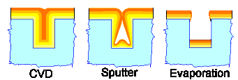
Coverage is not conformal! |
|
|
| |
| |
 |
Ion implantation |
|
|
|
 |
Depth (< ca. 1 µm) and dose precisely controllable. |
|
|
 |
Very compley and expensive | |
|
 |
Method od choice for making doped layers. |
|
|
 |
Introduces defects or destroys crystallinity Þ annealing
at high T (> 800 oC) is a must | |
| | |
| |
|
 |
There are many more techniques for producing thin layers |
|
 | | Comparing edge coverage |
|
|
 |
Evaporation. Relatively simple but limited as to materials and edgencoverage |
|
|
 |
Molecular beam epitaxy. (MBE) Standard for III-V's |
|
|
 |
Spin-on techniques ("Sol- Gel"). Used for making photo resist layers; occasionally
for others | |
|
 |
Galvanics. Kind of crude but necessary for Cu interconnects in modern IC's |
|
 |
| Edge coverage may be the decisive property! |
|
| |
| |
| |
 |
Structuring means selective removal of material (through a mask) by etching.
There are three main conditions for etching: | |
|
|
 |
1. Must attack material to be etched Þ
etching rate. | |
|
 |
2. Must not attack everything else Þ
selectivity. | |
|
 |
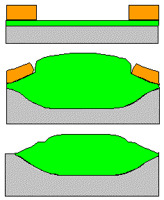
3. Must conserve structure of mask (good on left side of picture, not so good on right
side). | |
|
| |
| |
 |
Chemical etching: |
|
|
|
 |
Can be near perfect for points 1. and 2.. Example: HF attacks only SiO2
but not Si and most other materials. | |
|
 |
Fails miserably on point 3. |
|
|
 |
Underetching is unavoidable. Can't be used for lateral structure sizes < »
2 µm | |
| | |
| |
|
 |
Plasma etching ("Dry" etching) |
|
|
|
 |
In a plasma quite unusual reactions can take place - including reactions never seen in normal
chemistry. Many materials can be etched in a suitable plasma |
|
|
 |
Etching might preserve the lateral mask dimensions - for reasons not always entirely clear |
|
|
 |
There is tremendous potential in plasma etching because of the tremendously large parameter
space - and tremendous problems and costs for the same reasons |
|
|
 |
Allmost all "small" structures in semiconductor technology are obtained by plasma
etching | |
| |
| |
| |
 |
Lithography comprises three elementary steps: |
|
|
|
 |
Cover the layer to be structured with a light-sensitive layer called (photo)
resist | |
|
 |
Expose the resist to light only where you want the structure by a "slide projector"
called stepper (always demagnify the "slide" called reticle. |
|
|
 |
Develop the exposed resist in such a way that unexposed parts are etched off. |
|
|
 |
The structure has now be transferred into the resist; the process is rather similar to regular
old-fashioned analog photography. | |
| | |
| |
|
 |
The problem is that we want to make structures with lateral sizes in the 30
nm region, far smaller than the wavelength of light. This necessitates extreme measures in all components involved |
|
|
|
 |
At the core of lithography are the steppers - optical machines for around 5 Mio
€ a piece | |
|
 |
Resist technology, too, is a highly developed part of lithography |
|
|
 |
For some big problems simple solutions have been found. Example: reticles with pellicles |
| |
| |
|
© H. Föll (Semiconductor Technology - Script)
