 |
Integration means: | |
|
|
 |
1. Produce a large number (up to 1.000.000.000) of transistors
(bipolar or MOS) and other electronic elements on a cm2 of Si |
|
|
 |
2. Keep thoses elements electrically insulated from each other. |
|
|
 |
3. Connect those elements in a meaningful way to produce a system / product. |
|
| |
| |
| |
 |
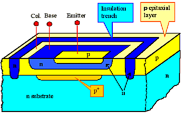
An integrated bipolar transistor does not resemble the textbook picture at all,
but looks far more complicated Þ. |
|
|
|
 |
This is due to the insulation requirements, the process requirements, and the need to interconnect
as efficiently as possible. | |
|
 |
The epitaxial layer cuts down on the number of critical diffusions, makes insulation easier,
and allows a "buried contact" structure. | |
| | |
| |
|
 |
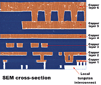
Connecting transistor / elements is complicated; it has to be done on several
levels | |
|
|
 |
Materials used are Al ("old"), Cu ("new"), W, (highly
doped) poly-Si as well as various silicides. | |
|
 |
Essential properties are the conductivity s of the conductor,
the dielectric constant er of the intermetal dielectric, and the resulting
time constant t = s · er
that defines the maximum signal transmision frequency through the conducting line. |
|
| |
| |
| |
 |
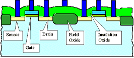
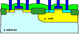
Integrating MOS transistors requires special measures for insulation (e.g.
a field oxide) and for gate oxide production | |
|
|
 |
Since a MOS transistor contains intrinsically a capacitor (the gate "stack"),
the technology can be used to produce capacitors, too. | |
| | |
| |
|
 |
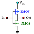
CMOS allows to reduce power consumption dramatically. |
|
|
|
 |
The process, however, is more complex: Wells with different doping type need to be made. |
|
| |
| |
| |
 |
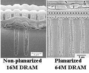
Using the third dimension (depth / height) might become necessary for integrating
"large" structures into a small projected are (example: trench capacitor in DRAMs Þ). |
|
|
|
 |
Unwanted "topology", however, makes integration more difficult. |
|
|
 |
Planarized technologies are a must since about 1995! Þ |
|
| |
| |
| |
 |
It ain't neither easy nor cheap! |
|
| Property | Number |
| Feature size | 0,2 µm |
| No. metallization levels | 4 - 7 |
| No. components | > 6 · 108 (Memory) |
| Complexity | > 500 Process steps |
| Cost (development and 1 factory) |
ca. $ 6 · 109 |
|
| | |
|
| |
| |
| |
| |
| |
| |
© H. Föll (Semiconductor Technology - Script)
