 |
Basic Considerations for Process Integration |
|  |
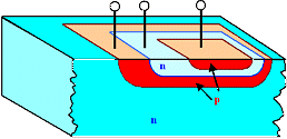
Draw a cross section of an integrated pnp-bipolar transistor! Denote in
the drawing all doping types and the purpose of the layers! |
|
 |
Compare an integrated bipolar transistor made with or without an epitaxial layer.
Describe advantages and problems of either approach. |
|
 |
Give a plot of the doping atom concentration as a function of depth for the kind of transistor
shown. Describe qualitatively but with rough numbers as far as possible
- Indicate the pn junctions in your drawing. Discuss their depth and distance in terms of process stability.
- Describe how the doping could be administered.
- Discuss possible problems encountered, in particular if the substrate doping is rather high.
|
|
|
|
 |
What function has a "buried layer" in bipolar technology? |
|
 |
Draw a cross section of two integrated p-MOSFET transistor! Denote in the
drawing the materials and the purpose of the decisive layers! Include typical lateral and vertical dimensions! Give key
requirements for the dielectrics! |
|
 |
Give a schematic drawing of a two-level metallization; make a list of the essential
process steps and enumerate the materials used in each step. |
|
 |
What exactly is a field oxide needed for? |
|  |
What is the difference between MOS and CMOS? 'Compare a MOS
and CMOS inverter for this. |
|
 |
Draw a schematic cross-section of two complementary MOS transistors next
to each other. Indicate the major difference to MOS. |
| |
| |
© H. Föll (Semiconductor Technology - Script)

![]() 5.4 Summary to 5: Integrated Circuits - Process Integration
5.4 Summary to 5: Integrated Circuits - Process Integration