| |
 |
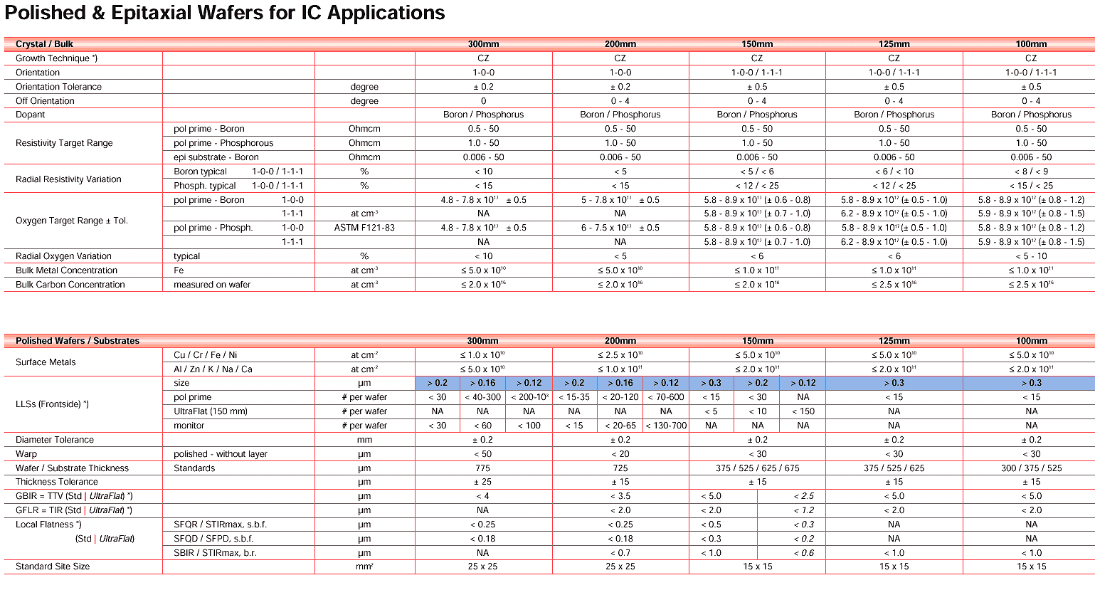
Here are the specification for Si wafers from one of the worlds top companies,
Wacker Siltronic, as they appear in the Internet in Nov. 2000. |
|
 |
Notice: Concentrations here are in cm–
3. The conversion to part per milion (ppm) is simple:orrelation |
|  |
The atomic density of Si is 4.96 · 1022 cm– 3 or
about 5 · 1022 cm– 3. This gives us |
|
|
|
|
 |
The lowest concentration given in the table (look for it) is 5 · 1010 cm–
3; it corresponds to 1 ppt
or 10– 12. |
|
 |
Surface concentrations [S] (given in cm– 2) are converted to volume concentrations [V] by |
| |
|
|
 |
With a = lattice constant (= 0,5431 nm) or, more precise for single crystals,
distance between the crystallographic planes. With a approximately 0,5 nm = 5· 10– 8
cm, we have
[V] = 5 · 1016 cm–3 = 1 ppm corresponds to S = 108 cm–
2 |
|
 |
Many specifications relate to the "flatness" of the wafers and the perfection of the surface;
the abbreviations used are
LLS
(sometimes also abbreviated LPDs): Localized Light Scattering
Defect; this relates to a detection method of sub-µm size surface imperfections (resulting from bulk microdefects)
SFQR
: Site flatness quality requirements (??): Whatever it means in detail - definitely a measure of flatness in a region comparable
to the size of a single chip. |
|
 |
(The rest: Who knows - to be included later) |
| | |
 |
© H. Föll (Semiconductors - Script)
