 |
We start from a (constant) distribution of positive charges (for n-doped
semiconductors) in the space charge region. |
|
 |
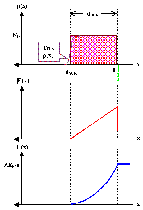
The corresponding negative charges are all on the surface; the charge distribution is shown
in the first frame of the illustration. |
|
 |
Poisson's equation states
that (for the one-dimensional case). |
| |
| e e0 |
d2 V(x)
dx2 |
= – |
r(x) | = |
e · ND |
|
|
|
 |
For 0 < x < dSCR and = 0 everywhere else. (We
can also use the voltage U(x) instead of V(x) if we think as V(x
= ¥) = 0). That will also be reflected in the choice of boundary conditions made below. |
 |
The drawing below shows the situation, including the slight approximation implicit in our choice
of r(x). Note that the x -direction ist to the left in this case. |
| |
|
|
 |
The first straight-forward integration yields dU/d( x) which is the electrical
field strength Ex = –dU/dx , or |
|
|
| ee0 |
dV( x)
dx |
= – e e0
Ex | = |
e · ND · x + const. |
|
|
|
 |
With the boundary condition Ex(x = dSCR ) = 0, we obtain
(always for the interval x = 0 and x = dSCR , of course): |
| |
| e ·ND · dSCR + const |
= | 0 |
| | |
| | const |
= |
– e ·ND · dSCR |
|
| Ex | = | 1
ee 0 | · |
(e · NDdSCR – e · ND · x) |
|
|
|
 |
The second integration yields |
|
|
| ee0 · U(x)
| = |
e · ND · x2
2 |
– e · ND · dSCR · x
+ const. |
|
|
|
 |
With the boundary condition U(dSCR) = 0, we obtain . |
| |
| – | e · ND · d
2SCR
2 |
+ const. | = | 0 |
| | | |
| | |
| | |
| const. |
= | e · ND · d
2SCR
2 |
|
|
|
 |
Using the proper expression for the integration constant gives gives us the complete voltage
function or the shape of the band bending |
| |
| ee0 · U(x)
| = |
e · ND · x2
2 | – |
e · ND · dSCR · x |
+ | e · ND · d
2SCR
2 |
|
|
|
 |
The width of the space charge region can be obtained by considering the voltage at x
= 0, where we have U( x = 0) = DE
F/e.Using this we obtain |
| |
ee0
e |
· DEF |
= | e · ND · d
2SCR
2 |
|
|
 |
This gives us the final result for the width of the space charge region |
| |
| dSCR | = |
1
e | · |
æ
ç
è |
2DEF · e
e0
ND |
ö
÷
ø | 1/2 |
|
|
 |
The corresponding curves are shown in the drawing above. We obtained the same formula as before, but now we have a better awareness of the approximations it contains.
|
|
 |
The positive charge distribution was assumed to be box-shaped and uniform. This is a rather good approximation;
the drawing indicates the precise shape of the charge distribution for comparison. |
|  |
The counter charges are described by a d
-function at the surface; these charges only enter the calculation in the indirect form of a boundary condition. |
|
|
© H. Föll (Semiconductors - Script)

![]() 2.2.4 Simple Junctions and Devices
2.2.4 Simple Junctions and Devices