 |
This is the case where an electrical field of arbitrary origin repulses the majority carriers
and a space charge region develops. |
|
 |
Starting with the Poisson equation for
doped semiconductors and all dopants ionized, we have |
|
|
d2(DEC)
dx2
| = – |
e2 · N
ee 0 |
æ
ç
è |
1 – | exp – |
DEC
kT |
ö
÷
ø |
|
|
|
 |
In contrast to the case of quasi-neutrality , we
now have +DEC >> kT and the sign is important! |
 |
This leads to a simple approximation: |
|
|
|
|
 |
The Poisson equation for the part of the semiconductor that contains this carrier density reduces to |
| |
d2(DEC)
dx2
| = – |
e2 · ND
ee 0 |
|
|
 |
We have treated this case already in the
more basic considerations. The result was |
| |
| U(x) | = |
e · ND
2ee
0 |
· x2 – 2dSCR · x + dSCR2 |
| dSCR | = |
1
e | · |
æ
ç
è |
2DEC(x = 0) · ee0
ND |
ö
÷
ø |
1/2 |
|
|
|
 |
With D EC(x = 0) = DE
for brevity, we can rewrite the expression for the width of the space charge layer in terms of the Debye length LDb |
| |
| LDb | = |
æ
ç
è |
e e0 · kT)
e2 · ND |
ö
÷
ø |
1/2 |
|
|
|
 |
and obtain |
| |
| dSCR | = |
LDb · |
æ
ç
è |
2DE
kT |
ö
÷
ø |
1/2 |
|
|
|
 |
If we express DE in terms of the the voltage U
between the ends of the sample by e · U = DE, we have the final result |
| |
| dSCR | = |
LDb · |
æ
ç
è |
2 · e · U
kT |
ö
÷
ø | 1/2 |
|
|
 |
Remember that LDb is a purely material related quality and thus a
constant for a given semiconductor. The width of the space charge region can be expressed
very simply in terms of LDb
, it is always larger by the factor {2eU/kT}1/2 |
|  |
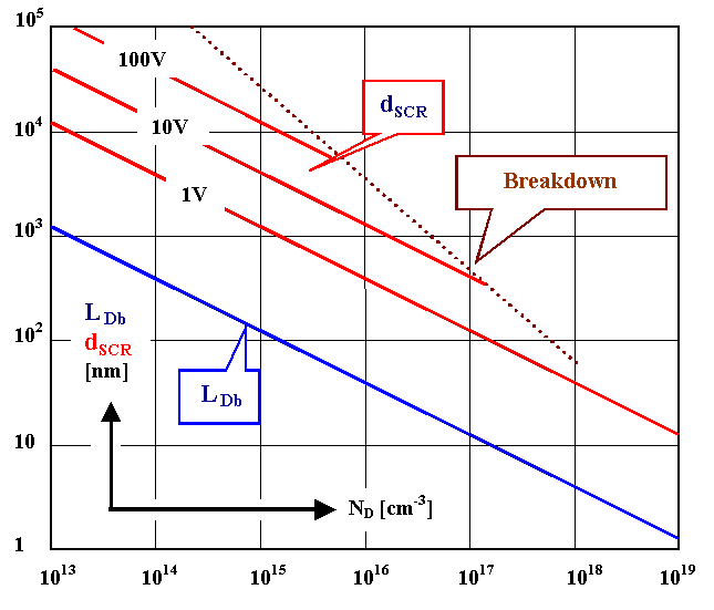
Since kT at room temperature » 1/40 eV, while applied
voltages may be up to 1000 V, dSCR may exceed LDn by several orders
of magnitude. This is shown in the illustration below (the numbers are basically correct, but not in detail). |
|
 |
The breakdown limit indicates that the SCR, being an dielectric insulator, will eventually experience
electrical breakdown if the field
strength exceeds an upper limit. |
| |
|
| |
|
© H. Föll (Semiconductors - Script)

![]() Space Charge Region and Poisson Equation
Space Charge Region and Poisson Equation ![]() Band-Bending and Surface Charge
Band-Bending and Surface Charge