 |
As you know, the first law of Materials
science is "Everything can be broken".
Dielectrics are no exception to this rule. If you increase the voltage applied to a capacitor, eventually you will produce
a big bang and a lot of smoke - the dielectric material inside the capacitor will have experienced "electrical breakdown" or electrical break-through, an irreversible and practically always destructive
sudden flow of current. |
|
 |
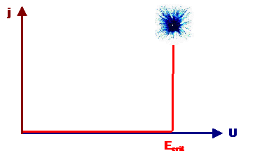
The critical parameter is the field strength E in the dielectric. If it is too
large, breakdown occurs. The (DC)
current vs. field strength characteristic of a dielectric therefore may look look this: |
| |
|
|
 |
After reaching Ecrit, a sudden flow of current may, within very short times (10–8
s) completely destroys the dielectric to a smoking hot mass of undefinable structure. |
|  |
Unfortunately, Ecrit is not a well defined
material property, it depends on many parameters, the most notable (besides the basic material itself) being the production
process, the thickness, the temperature, the internal structure (defects and the like), the age, the environment where it
is used (especially humidity) and the time it experienced field stress. |
 |
In the cases where time plays an essential role, the expression "failure"
is used. Here we have a dielectric being used at nominal field strength well below its breakdown field-strength for some
time (usually many years) when it more or less suddenly "goes up in smoke". Obviously the breakdown field strength
decreases with operating time - we observe a failure of the material. |
|
 |
In this case the breakdown may not be explosive; but a leakage current may develop which grows over time
until a sudden increase leads to total failure of the dielectric. |
|
 |
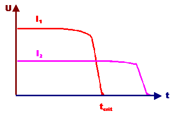
The effect can be most easily tested or simulated, by impressing a constant (very
small) current in the dielectric and monitoring the voltage needed as a function of time. Remember that by definition
you cannot have a large current flowing through an insulator = dielectric; but "ein bißchen was geht immer"
- a tiny little current is always possible if you have enough voltage at your disposal. A typical voltage-time curve may
then look like this: |
| |
|
|
 |
The voltage needed to press your tiny test current through the dielectric starts to decrease
rapidly after some time - hours, days, weeks, ..., and this is a clear indication that you dielectric becomes increasingly
leaky, and will go up in smoke soon. |
|
 |
A typical result is that breakdown of a "good" dielectric occurs after - very roughly
- 1 C of charge has been passed. |
 |
The following table gives a rough idea of critical field strengths for certain
dielectric materials |
| |
| Material |
Critical Field Strength
[kV/cm] | | Oil |
200 | | Glass, ceramics | 200...400 | | Mica | 200...700 |
| Oiled paper | 1800 | | Polymers | 50...900 |
| SiO2 in ICs | > 10 000 |
|
 |
The last examples serves to remind you that field strength
is something totally different from voltage! Lets look at typical data from an integrated
memory circuit, a so- called DRAM , short for Dynamic Random Access Memory.
It contains a capacitor as the central storage device (no charge = 1; charge = 0). This capacitor has the
following typical values: |
|
 |
Capacity
» 30 fF (femtofarad)
Dielectric:
ONO, short
for three layers composed of Oxide (SiO2), Nitride (Si3N4 ) and Oxide again
- together about 8 nm thick!
Voltage: 5 V, and consequently
Field strength
E = 5/8 V/nm » 6 · 106 V/cm. |
|  |
This is far above the critical field strength for practically all bulk materials! We see very graphically that high field strength and voltage have nothing to
do with each other. We also see for the first time that materials in the form of a thin film
may have properties quite different from their bulk behavior - fortunately they are usually much "better". |
 |
Last, lets just note in passing, that electrical breakdown is not
limited to insulators proper. Devices made from "bad " conductors - i.e. semiconductors
or ionic conductors - may contain regions completely depleted of mobile carriers - space charge regions at junctions are one example.
|
|
 |
These insulating regions can only take so much field strength before they break down, and this may severely
limit their usage in products |
| |
|
© H. Föll (Electronic Materials - Script)

