 |
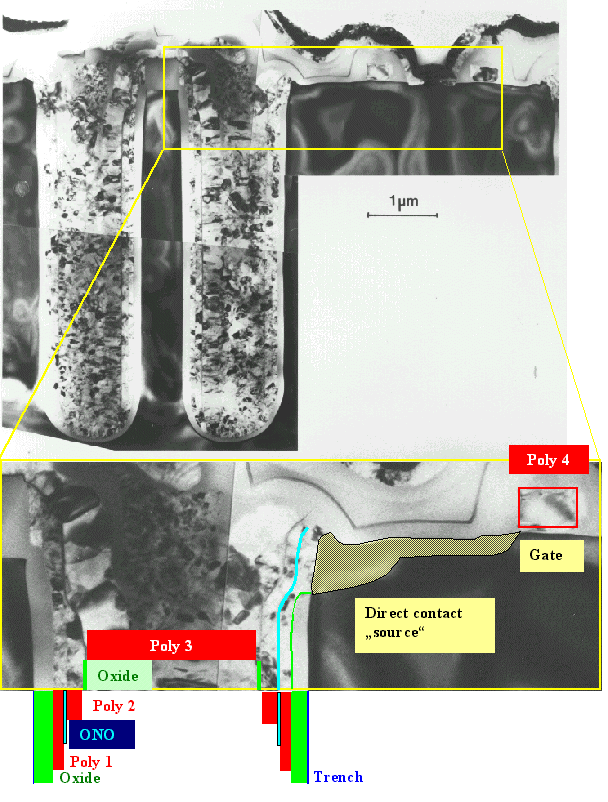
Here is a large size rendering of the TEM picture of a 16 Mbit DRAM
memory cell. A drawing of this cross section can be found in
the link. |
| |
|
 |
.Many details are not visible in this low magnification picture. Below we see
the ONO layer between the two poly Si layers at high magnification |
|
 |
The two oxide layers appear white; the nitride layer dark |
| |
|
 |
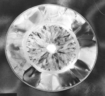
Next, we look at a trench capacitor "from above"
and not in cross section. |
|
 |
Shown is the "simple" capacitor from the 4 Mbit DRAM generation. ONO
us used as dielectric; and the substrate Si served as one electrode. |
|
 |
Again the poly electrode was oxidized for insulation and the trench filled with poly. The
smaller (and dendritic) grain structure indicates that a large deposition rate (at somewhat higher pressure) was used; and
a little hole remained unfilled in this case. |
| |
|
© H. Föll (Electronic Materials - Script)


![]() 6.3.3 CVD for Poly-Silicon, Silicon Nitride and Miscellaneous Materials
6.3.3 CVD for Poly-Silicon, Silicon Nitride and Miscellaneous Materials ![]() Cross Section of 16 Mbit DRAM and 64 Mbit DRAM
Cross Section of 16 Mbit DRAM and 64 Mbit DRAM