 |
You have a trench (i.e. in reality
a hole) with a diameter of about 1 µm
and a depth of 5 µm. The Si around it serves as one of the capacitor electrodes and must be doped
with something to a depth of about 0,3 µm so it is highly conductive. |
|
 |
This task came up as an unprecedented challenge to process engineers in the context
of the 4 Mbit DRAM generation around 1985. How do you do it? |
 |
First you try what you have - ion implantation - and hope for the best. Since
the ion beam does not impinge at right angels on the specimen, but somewhat off (say about 10o) for various
reasons, there is hope. |
|
 |
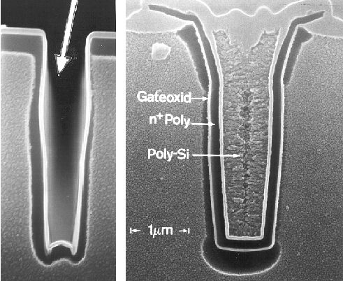
Indeed, it works - see below: |
| |
|
 |
With a special etchant the doped region is etched off, leaving a dark rim around
the trench (which was not very perfectly etched at this point in time). |
|
 |
The arrow in the left-hand picture marks the major direction of the ion beam, and the left-hand
side of the trench is nicely doped, as one would expect. The right hand picture shows a fully processed trench capacitor
for measurements of the electrical characteristics. |
|
 |
But some implantation also took place on the unfavorable side - there is a certain spread
in the beam angle, some ions are reflected or scattered off their original direction - whatever happens, some ions hit the
wall. If you turn the wafer during implantation, it might be possible after all, to obtain decent homogeneous doping. |
|
 |
But in the end, ion implantation was not used. Too expensive, too dependent on the precise
trench geometry (which changes all the time), simply not good enough for prolonged mass production. |
| |
 |
How? Well, let's deposit a "spin-on
glass" (SOG)containing
the dopant, hope that it will completely fill the trenches, and then diffuse the dopant out of the SOG into the Si. |
|
 |
Spin-on glasses are used a lot, but do they fill up fine holes? The only way
to find out is trying it. |
|
 |
To cut a long story short - it worked. But not reliably enough; didn't make it to production. |
 |
What finally made it to production is a somewhat similar approach, except that
the SOG was replaced by an As doped TEOS-oxide. |
|
 |
Not an extremely nice process (the coating of the CVD tube is As contaminated
and highly toxic), but without many unknowns and reproducibly. |
 |
Is there something even better? |
|
 |
Yes, there is a simple solution to the trench doping problem: Don't
do it. Oxidize the trench walls and deposit a layer of highly doped poly-Si as the capacitor electrode.
Simple. Elegant. |
|
 |
Except that now you have to produce the very thin capacitor dielectric on poly-Si.
Thermal oxidation of poly-Si will not be good enough - now
you need ONO. The result was already shown
in an illustration module |
| |
|
© H. Föll (Electronic Materials - Script)
