 |
Micromechanical devices made from Si are rapidly gaining in importance.
Their production process utilizes most everything used in microelectronics, plus a few special processes. |
 |
Again, we will not discuss MEMS in this Hyperscript, but show only a few
pictures of what can be made. |
|
 |
Let's look at mechanical
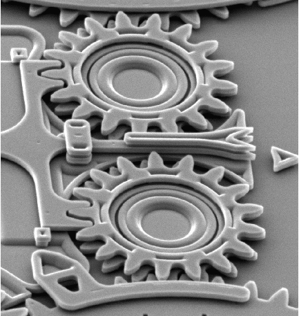
MEMS first. On top, a microscopic gear wheel systems from Sandia Labs. It could
be used for mechanically "locking" your computer; which might be more secure than just software protection.
|
|
 |
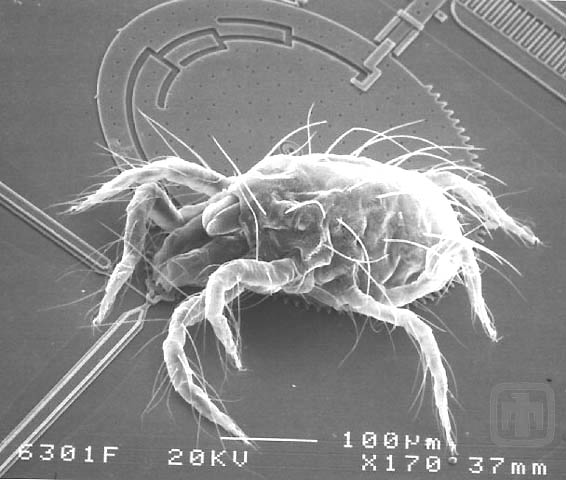
On the bottom, more or less the same thing with a dust mite on it. This is the
little animal that lives in your rug, bed and upholstery and gives a fair share of us the infamous dust ("Hausstaub")
allergy |
| |
 |
 |
Pictures: Courtesy of Sandia National Laboratories,
SUMMiTTM Technologies, www.mems.sandia.gov"
|
|
|
 |
While gear wheels look very good, the real use of MEMS so far is in sensors, in particular
for acceleration. The sensor exploding your air bag when you wrap your car around a tree is the paradigmatic MEMS
product. |
 |
If we look at optical
MEMS, we are mostly also looking on a mechanical microstructure, in this case at arrays of little mirrors which can
be addresses individually and thus "process" a light beam pixel by pixel. |
| |
 |
 |
Courtesy of "ISiT"
(Fraunhofer Institut Silizium Technologioe; Itzehoe, Germany) |
Courtesy of Texas Instruments |
|
|
 |
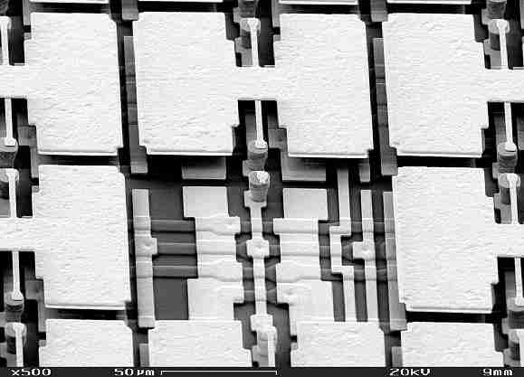
On the left we have an array of microscopic mirrors that can be moved up and down electrically
(from the ISiT in Itzehoe). The central mirror is removed to show the underlying structure |
|
 |
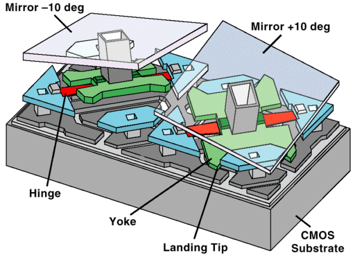
On the right a schematic drawing of the "mechanical" part of Texas Instruments ("DLP"
= digital light processing) chip, the heart of many beamers. |
|
 |
But many other things are possible with MEMS, suffice it to mention "bio-chips",
micro-fluidics, sensors and actuators for many uses, microlenses and lens arrays, and tunable capacitors and resonators,
and, not to forget, very down-to-earth products like the micro-nozzles for ink jet printers. |
| |
|
 |
There are many more applications, most in the development phase, that exploit
the exceptional quality of large Si crystals, the unsurpassed technology base for processing, or simple emerging
new features that might be useful. Here are few examples: |
 |
While there are no conventional lenses for X-rays or neutron beams, some
optics is still possible by either using reflection (i.e. imaging with mirrors) or diffraction. |
|
 |
An good X-ray mirror, like any mirror, must have a roughness far smaller
than the wavelength. For useful applications (like "EUV" = Extreme Ultraviolet) lithography (it is really
X-ray lithography, but this term has been "burned" in the 80ties and is now a dirty word in microelectronics),
this quickly transfers into the condition that the mirrors must be more or less atomically flat over large areas. This can
be only done with large perfect single crystals, so your choice of materials is no choice at all: You use Si. |
|
 |
If you want to "process" a neutron beam, e.g. to make it monochromatic,
you use Bragg diffraction at a "good" crystal. Again, mostly only large and perfect single crystals of Si
meet the requirements |
 |
Si is fully transparent for IR light and is thus a great material for making
IR optics. In this field, however, there is plenty of competition from other materials. But Si is the material
of choice for mirrors and prisms needed for IR spectroscopy. |
 |
Since about 1990 "porous Si" is emerging as a totally
new kind of material. It is electrochemically made form single-crystalline Si and comes in many variants with many,
partially astonishing properties (optically activity, highly explosive, ...) |
|
 |
A review about this stuff can be found in the link
. Here we simply note that a number of projects explores possible uses as for example electrodes for fuel cell, very special
optical and X-ray filters, biochips, fuses for airbags, "normal" and biosensors, or special actuators. |
| |
|
© H. Föll (Electronic Materials - Script)
