 |
When we make a contact to the structures in the Si, for example to source and
drain regions, we first cover everything with an insulator - SiO2 - and then make contact holes in the
proper places. Use the link to refresh your memory. |
|
 |
Next we cover everything with a metal - if we stay simple we just use Al.
We have a lot of other processes after that, and we will have to heat up the wafer to some extent for doing whatever needs
to be done. |
 |
What happens if we bring Si in contact with Al (or any other metal,
for that matter) and heat it up to some extent? |
|
| |
| |
|
 |
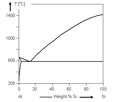
Well - consult the phase diagram, and it will tell you what you should expect
at whatever temperature you chose. Here is the Al - Si phase diagram. |
| |
 |
What it tells us it that somewhat below 600 oC we will have an eutectic. |
| |
 |
In other words, above the eutectic temperature, "things" will melt. Consult the
chapter about phase diagrams if you don't know exactly
what "things" means. |
|
|
 |
In yet other words, after Al deposition, we must not raise the temperature above the
eutectic temperature ever In order to stay on the safe side, we must even keep it below about 500 oC |
| |
 |
This is not so good, but something else is worse: The solubility of Si in Al
around 500 oC is finite - about 2 % one would estimate - , while at room temperature it is practically
nil. |
| |
| |
|
 |
So what happens if you heat up Al in contact to Si? The Al
will try to incorporate some Si; it will sort of "suck it up" from the Si substrate. |
| |
|
|
|
|
 |
In more scientific terms we talk about Si atoms diffusing into the Al (and Al
atoms diffusing into the Si); so temperature dependent quantities like diffusion coefficients are involved. |
| | |
 |
If we now have some of the Si
in the Al, it must be missing somewhere else; obviously right below the Al-Si interface we must expect
some "missing" Si. |
| |
|
 |
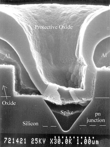
If we are lucky, the "missing" Si is uniformly distributed, i.e. the whole
surface of the Si moved down a bit. However, Murphy's law (What can go wrong will go wrong) applies, and on occasion
all the Si moving into the Al comes from one rather localized spot at the interface - we get a "spike".
This is shown very drastically in the picture. |
| |
|
 |
At the same time, Al will diffuse in the room left by the Si - our spike is
filled with Al and we have a short-circuited pn-junction! |
| | |
| |
 |
This ain't so good. Remember: One spike / short circuit in just one of the >
50 million or so contact holes will kill the whole IC. We must fix that problem. |
|
 |
Easy, you say. (Do you see the obvious solution?). We do not use pure Al,
but Al already containing some Si, so it does not have to "steal" Si from the substrate to
meet its solubility needs at higher temperatures. |
|
 |
Right. That is exactly what we will do. We use Al alloyed with 0.5%
- 1 % of Si. No more spikes will form, and as the process engineer in charge you can sleep well again at night.
|
 |
Really? Yes, you will. For a few years at least. But then you slumber will become
unruly again, because as dimensions shrink, you run into new problem. |
| | |
 |
You use Al(0.7 % Si) as your contact material. The dictate of the phase
diagram with regard to the Aluminium needs of Si at your highest temperature are met; no spiking will occur. |
|
 |
How about the needs of the Al at room temperature? They are not met, because
Si solubility at room temperature is negligible. |
|
 |
The phase diagram now dictates that Si precipitates should form. This will
need some nucleation and may be kinetically difficult in the bulk of the Al, but at the Al-Si interface we
already have Si and nucleation is easy. |
 |
In essence, we must expect the reverse of the "sucking Si into Al"
process to take place. The Al will "spit out" its surplus Si and deposit it right at the interface
|
|
 |
Si precipitates will grow epitaxially
(there is no reason why not) on the Si below the Al. We must expect to find some Si islands on top
of the Si |
| |
|
 |
That is exactly what we see in the pictures above. |
|
 |
In the left hand picture we have a nice balance of a few shallow spikes and some
Si precipitates following the contours of the grain boundaries in the Al (which has been etched off). This
is not surprising, because precipitation is a diffusion process, after all, and diffusion along grain boundaries is faster
then in the bulk. |
|
 |
The right hand picture shows rather large precipitates, almost taken up all the
space there is in the contact hole. |
 |
The question, of course, is: Does it matter? We still have some Al in contact
to our Si substrate, and than we have Al in contact to the Si precipitates and the Si precipitates
in contact to the Si substrate. Plenty of possibilities to run a current through the contact. |
|
 |
Right, but Al in Si is an acceptor, and we must expect the Si
precipitates to be saturated with Al and thus heavily p-doped. |
| | |
|
|
|

 |
 |
No big problem as long as the Si below the contact is p-doped,
too, but a big problem for n-doped Si and small contacts. |
| | |
 |
In this case part of the contact area is now a pn-junction, blocking current flow in
one direction. |
| |
|
 |
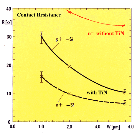
It is clear that the contact resistance always increases
with decreasing contact area, but if we have p-doped Si precipitates, we have only part of the geometrical
contact area for the contact to n-type Si. |
| | |
 |
What we get as a function of the contact hole size for the n-doped case is shown in
the figure in red. |
| |
|
 |
The message is clear: Contact resistance will be too large at some point. So what do you do? |
| |
| |
|
 |
Without the Si, you get spikes, with the Si you get precipitates
and a contact resistance that is too large. |
|
 |
There is no choice anymore: You need a new material; in this case a diffusion
barrier between the Si and the Al. |
 |
Introduce, e.g., a thin layer of Ti/TiN between the Si and the Al,
and your contact resistance problems are solved, as seen in the figure. If you also throw in contact
hole filling with W-CVD, you now have a structure like the one on the title
page. |
|
 |
Except, of course, that now you have to worry about how to make and structure
this layer. How to measure how thick it is, and if it has the required properties (assuming that you know that). |
|
 |
You must worry if the new diffusion barrier interferes with the reliability of
the metallization (after all, electromigration in the metal is one of the major
causes of premature device failures), and if can keep the additional processes cheap. |
 |
In other words. Introducing a new material is a long and cumbersome process. |
|
 |
And a frustrating one. Nobody tells you, that TiN is it! You (meaning you
and your team) find that out yourself. And in that process you will test many materials, most of which will not be the right
ones. |
|
 |
Out they go - and with them many hours of your time and a lot of (other peoples)
money. |
| |
|
© H. Föll (Electronic Materials - Script)


![]() 6.4.1 Physical Processes for Layer Deposition
6.4.1 Physical Processes for Layer Deposition