 |
Consider making a contact hole through the CVD oxide that was deposited
over the finished transistors. |
|
 |
Since the source/drain area are as small as possible, you have to make not only
a small hole but you must align it precisely relative to the gate stack of the transistors. |
|
 |
Small misalignements would produce a short circuit between the gate electrode and the Al
that will be put in the contact hole eventually. |
 |
Now cover the whole gate stack with Si3N4 that will
resist whatever etching procedure you use to remove the oxide in the future contact hole. You gain a lot in your "process window" for the contact hole - misalignements don't matter as much any more
as shown below. |
| |
|
 |
That looks pretty good - but there is a prize to pay: |
|
 |
First of all - how do we make the nitride encapsulation? And don't forget; Si3N4
must never come in contact with Si - you always need a thin layer of buffer
oxide underneath (not shown in the picture). There is quite a bit of added process complexity! |
|
 |
The topography gets worse. The aspect ratio of the contact hole - the relation between depth
and diameter - increases and with it the problems of filling it with Al. |
|
 |
Still, starting around 1987, FOBIC was used and helped to get the next generation
onto the market. |
 |
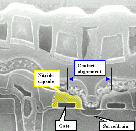
The picture below is a cross section through a 16 Mbit DRAM memory cell
shown before. It shows one of the contacts to a transistor
(which is connected on the other side to a trench capacitor).
The FOBIC structure has been outlined; it is clearly visible. |
| |
|
© H. Föll (Electronic Materials - Script)

